


61200214L1-1 IQ Probe User Manual 111
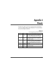
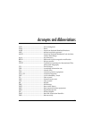
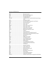
Appendix A. Pinouts
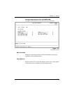
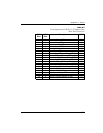
Table A-F
Pin Assignments for DB-25 to V.35 Adapter Cable
(Rear Panel Connector)
DB25
Pin#
V.35
Pin#
Description CCITT
1 A Protective Ground (PG) 101
2 P Transmitted Data (SD-A) 103
3 R Received Data (RD-A) 104
4 C Request to Send (RTS) 105
5 D Clear to Send (CTS) 106
6 E Data Set Ready 107
7 B Signal Ground (SG) 102
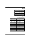
8 F Received Line Si
g
nal Detector
(
CD
)
109
9 X Receiver Si
g
nal Element Timin
g
(
SCR-B
)
115
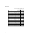
11 W External TX Si
g
nal Element
(
SCX-B
)
113
12 AA Transmitter Signal Element Timing (SCT-B) 114
13 V Receiver Signal Element Timing (SCR-A) 115
14 S Transmitted Data (SD-B) 103
15 Y Transmitter Signal Element Timing (SCT-A) 114
16 T Received Data (RD-B) 104
17 V Receiver Signal Element Timing (SCR-A) 115
18 J Ring Indicator (RI) -
19 P Transmitted Data (SD-A) 103
20 H Data Terminal Ready (DTR) -
21 BB
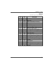
24 U External TX Signal Element (SCX-A) 113
25 K