


2000h
FFFFh
0000h
1FFFh
40 43 EA
41 44 PSEN
42 45 ALE
43 46 P0.0 / AD0
44 47 P0.1 / AD1
45 48 P0.2 / AD2
46 49 P0.3 / AD3
47 50 DGND
48 51 DVDD
49 52 P0.4 / AD4
50 53 P0.5 / AD5
51 54 P0.6 / AD6
52 55 P0.7 / AD7
27 29 MOSI / D1
28 30 P2.0 / A8 / A16
29 31 P2.1 / A9 / A17
30 32 P2.2 / A10 / A18
31 33 P2.3 / A11 / A19
32 34 XTAL1 (in)
33 35 XTAL2 (out)
34 36 DVDD
35 37,38 DGND
36 39 P2.4 / A12 / A20
37 40 P2.5 / A13 / A21
38 41 P2.6 / A14 / A22
39 42 P2.7 / A15 / A23
14 16 MISO
15 17 RESET
16 18 P3.0 / RxD
17 19 P3.1 / TxD
18 20 P3.2 / INT0
19 21 P3.3 / INT1
20 22 DVDD
21 23 DGND
22 24 P3.4 / T0
23 25 P3.5 / T1
24 26 P3.6 / WR
25 27 P3.7 / RD
26 28 SCLOCK / D0
1 56 P1.0 / T2
2 1 P1.1 / T2EX
3 2 P1.2 / IEXC1 / DAC
4 3 P1.3 / IEXC2 / AIN5
5 4,5 AVDD
6 6,7,8 AGND
7 9 REFIN-
8 10 REFIN+
9 11 P1.4 / AIN1
10 12 P1.5 / AIN2
11 13 P1.6 / AIN3
12 14 P1.7 / AIN4 / DAC
13 15 SS
ADD A,source 1,2 12
add source to A
ADD A,#data 2 12
ADDC A,source 1,2 12
add with carry
ADDC A,#data 2 12
SUBB A,source subtract from A 1,2 12
with borrow
SUBB A,#data 2 12
INC A 1 12
INC source increment 1,2 12
INC DPTR * 1 24
DEC A 1 12
decrement
DEC source 1,2 12
MUL AB multiply A by B 1 48
DIV AB divide A by B 1 48
DA A decimal adjust 1 12
MOV A,source 1,2 12
MOV A,#data 2 12
MOV dest,A move source 1,2 12
to destination
MOV dest,source 1,2,3 24
MOV dest,#data 2,3 12,24
MOV DPTR,#data16 3 24
MOVC A,@A+DPTR move from 1 24
code memory
MOVC A,@A+PC 1 24
MOVX A,@Ri 1 24
MOVX A,@DPTR move to/from 1 24
data memory
MOVX @Ri,A 1 24
MOVX @DPTR,A 1 24
PUSH direct push onto stack 2 24
POP direct pop from stack 2 24
XCH A,source exchange bytes 1,2 12
XCHD A,@Ri exchg low digits 1 12
ACALL addr11 2 24
call subroutine
LCALL addr16 3 24
RET return from sub. 1 24
RETI return from int. 1 24
AJMP addr11 2 24
LJMP addr16 3 24
jump
SJMP rel 2 24
JMP @A+DPTR 1 24
JZ rel jump if A = 0 2 24
JNZ rel jump if A not 0 2 24
CJNE A,direct,rel 3 24
CJNE A,#data,rel compare and 3 24
jump if not
CJNE Rn,#data,rel equal 3 24
CJNE @Ri,#data,rel 3 24
DJNZ Rn,rel decrement and 2 24
jump if not zero
DJNZ direct, rel 3 24
NOP no operation 1 12
CLR C 1 12
clear bit to zero
CLR bit 2 12
SETB C 1 12
set bit to one
SETB bit 2 12
CPL C 1 12
complement bit
CPL bit 2 12
ANL C,bit AND bit with C 2 24
ANL C,/bit ...NOTbit with C 2 24
ORL C,bit OR bit with C 2 24
ORL C,/bit ...NOTbit with C 2 24
MOV C,bit 2 12
move bit to bit
MOV bit,C 2 24
JC rel jump if C set 2 24
JNC rel jmp if C not set 2 24
JB bit,rel jump if bit set 3 24
JNB bit,rel jmp if bit not set 3 24
JBC bit, rel jmp&clear if set 3 24
ANL A,source 1,2 12
ANL A,#data 2 12
logical AND
ANL direct,A 2 12
ANL direct,#data 3 24
ORL A,source 1,2 12
ORL A,#data 2 12
logical OR
ORL direct,A 2 12
ORL direct,#data 3 24
XRL A,source 1,2 12
XRL A,#data 2 12
logical XOR
XRL direct,A 2 12
XRL direct,#data 3 24
CLR A clear A to zero 1 12
CPL A complement A 1 12
RL A rotate A left 1 12
RLC A ...through C 1 12
RR A rotate A right 1 12
RRC A ...through C 1 12
SWAP A swap nibbles 1 12
Rn register addressing using R0-R7
direct 8bit internal address (00h-FFh)
@Ri indirect addressing using R0 or R1
source any of [Rn, direct, @Ri]
dest any of [Rn, direct, @Ri]
#data 8bit constant included in instruction
#data16 16bit constant included in instruction
bit 8bit direct address of bit
rel signed 8bit offset
addr11 11bit address in current 2K page
addr16 16bit address
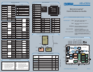
ADuC824
MicroConverter
®
Quick Reference Guide
EQU define symbol
DATA define internal memory symbol
IDATA define indirect addressing symbol
XDATA define external memory symbol
BIT define internal bit memory symbol
CODE define program memory symbol
DS reserve bytes of data memory
DBIT reserve bits of bit memory
DB store byte values in program memory
DW store word values in program memory
ORG set segment location counter
END end of assembly source file
CSEG select program memory space
XSEG select external data memory space
DSEG select internal data memory space
ISEG select indirectly addressed internal
data memory space
BSEG select bit addressable memory space
external
program
memory
EA=1
internal
8K bytes
Flash/EE
EA=0
external
PRINTED IN U.S.A. G02077-2.5-02/02 (A)
* INC DPTR increments the 24bit value DPP/DPH/DPL
Interrupt
Bit
Interrupt Name
Vector
Address
Priority
within
Level
PSMCON.5 Power Supply Monitor Interrupt 43h 1
WDS WatchDog Timer Interrupt 5Bh 2
IE0 External Interrupt 0 03h 3
RDY0/RDY1 End of ADC Conversion Interrupt 33h 4
TF0 Timer0 Overflow Interrupt 0Bh 5
IE1 External Interrupt 1 13h 6
TF1 Timer1 Overflow Interrupt 1Bh 7
ISPI SPI Interrupt 3Bh 8
RI/TI UART Interrupt 23h 9
TF2/EXF2 Timer2 Interrupt 2Bh 10
TIMECON.2 Time Interval Counter Interrupt 53h 11
(256 counts
per
o
C)
200µA / 400µA
AIN
MUX
16bit
counter
timers
DAC
control
ADC
control
&
calibration
DAC
OSC &
PLL
bandgap
reference
TEMP
sensor
time
interval
counter
V
REF
detect
AIN
MUX
ADC
control
&
calibration
24 bit
Σ∆ ADC
(primary ADC)
(auxillary ADC)
16 bit
Σ∆ ADC
power supply
monitor
synchronous
serial interface
(SPI)
8K x 8
program
Flash/EE
640 x 8
data
Flash/EE
watchdog
timer
256 x 8
user RAM
asynchronous
serial port
(UART)
8052
MCU
core
downloader
debugger
PGABUF
BUF
single-pin
emulator
ADuC824
9
10
11
12
8
7
2
1
23
22
3
26
27
14
32
33
25
24
23
22
19
18
17
16
39
38
37
36
31
30
29
28
12
11
10
9
4
3
2
1
52
51
50
49
46
45
44
43
42
41
40
15
18
19
5
6
20
34
35
47
21
48
AIN1
AIN2
AIN3
AIN4
REFIN+
REFIN-
INT1
INT0
T2EX
T2
T1
T0
DAC
AV
DD
AGND
SCLOCK
MOSI
MISO
ALE
PSEN
EA
RESET
XTAL1
XTAL2
DV
DD
DGND
13SS
3
4
I
EXC
1
I
EXC
2
P3.7
P3.6
P3.5
P3.4
P3.3
P3.2
P3.1
P3.0
P2.1
P2.0
P1.7
P1.6
P1.5
P1.4
P1.3
P1.2
P1.1
P1.0
P0.7
P0.6
P0.5
P0.4
P0.3
P0.2
P0.1
P0.0
P2.2
P2.3
P2.4
P2.5
P2.6
P2.7
16
17
RxD
TxD
4AIN5
18
19 INT1
INT0
26
27 D1
D0
26
25
24
23
22
21
20
19
18
17
16
15
14
40
41
42
43
44
45
46
47
48
49
50
51
52
13
12
11
10
9
8
7
6
5
4
3
2
1 39
38
37
36
35
34
33
32
31
30
29
28
27
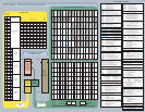
ADuC824
52pin PQFP
TOP VIEW
(not to scale)
pin 1 identifier
Arithmetic Operations
bytes
OSC
periods
bytes
OSC
periods
Data Transfer Operations
Logical Operations
Boolean Variable ManipulationProgram Branching
bytes
OSC
periods
bytes
OSC
periods
bytes
OSC
periods
INSTRUCTION SET
Legend
PROGRAM MEMORY SPACE (read only)
ASSEMBLER DIRECTIVES
INTERRUPT VECTOR ADDRESSES
PIN FUNCTIONS
FUNCTIONAL BLOCK DIAGRAM
64K bytes
addressable
a “Data Acquisition System on a Chip”
ADC: 24bit Σ∆ with programmable gain,
plus 16bit Σ∆ auxiliary ADC
DAC: 12bit, 15µs, voltage output, rail-to-rail
<1LSB DNL
EEPROM: 8K bytes Flash/EE program memory
640 bytes Flash/EE data memory
microcontroller: industry standard 8052
32 I/O lines, programmable PLL clock
(98KHz to 12MHz from 32KHz crystal)
other on-chip features: calibrated temperature sensor, power supply
monitor, watchdog timer, flexible serial
interface ports, voltage reference, time interval
counter
the ADuC824 is:
www.analog.com/microconverter REV. A
26
25
24
23
22
21
20
19
18
17
16
15
28
54
55
56
43
44
45
46
47
48
49
50
51
52
13
12
11
10
9
8
7
6
5
4
3
2
1
39
38
37
36
35
34
33
32
31
30
29
42
41
ADuC824
56pin CSP
TOP VIEW
(not to scale)
pin 1 identifier
14
40
27
53
PQFP
CSP
P3.7 (RD)
P3.6 (WR)
P3.5 (T1)
P3.4 (T0)
P3.3 (INT1)
P3.2 (INT0)
P3.1 (TxD)
P3.0 (RxD)
P2.1 (A9 / A17)
P2.0 (A8 / A16)
P1.7 (AIN4 / DAC)
P1.6 (AIN3)
P1.5 (AIN2)
P1.4 (AIN1)
P1.3 (I
EXC
2 / AIN5)
P1.2 (I
EXC
1 / DAC)
P1.1 (T2EX)
P1.0 (T2)
P0.7 (AD7)
P0.6 (AD6)
P0.5 (AD5)
P0.4 (AD4)
P0.3 (AD3)
P0.2 (AD2)
P0.1 (AD1)
P0.0 (AD0)
P2.2 (A10 / A18)
P2.3 (A11 / A19)
P2.4 (A12 / A20)
P2.5 (A13 / A21)
P2.6 (A14 / A22)
P2.7 (A15 / A23)