System Control Coprocessor
ARM DDI 0363E Copyright © 2009 ARM Limited. All rights reserved. 4-69
ID013010 Non-Confidential, Unrestricted Access
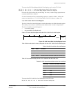
To access the nVAL Debug Request Enable Clear Register, read or write CP15 with:
MRC p15, 0, <Rd>, c15, c1, 7 ; Read nVAL Debug Request Enable Clear Register
MCR p15, 0, <Rd>, c15, c1, 7 ; Write nVAL Debug Request Enable Clear Register
On reads, this register returns the current setting. On writes, overflow debug requests that are
currently enabled can be disabled.
For more information of how to enable debug requests on counter overflows, and how the
requests are signaled, see c15, nVAL Debug Request Enable Set Register on page 4-64.
c15, nVAL Cache Size Override Register
The nVAL Cache Size Override Register overwrites the caches size fields in the main register.
This enables you to choose a smaller instruction and data cache size than is implemented.
The nVAL Cache Size Override Register is:
• a write-only register
• only accessible in Privileged mode.
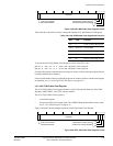
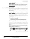
Figure 4-52 shows the bit arrangement for the nVAL Cache Size Override Register.
Figure 4-52 nVAL Cache Size Override Register format
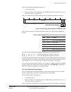
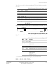
Table 4-50 shows how the bit values correspond with the nVAL Cache Size Override Register.
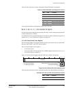
Table 4-51 shows the encodings for the nVAL instruction and data cache sizes.
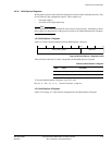
To access the nVAL Cache Size Override Register, write CP15 with:
MCR p15, 0, <Rd>, c15, c14, 0 ; nVAL Cache Size Override Register
Icache
31 16 15 78430
Reserved
Dcache
Table 4-50 nVAL Cache Size Override Register
Bits Field Function
[31:8] Reserved SBZ.
[7:4] Dcache Defines the nVAL data cache size. See Table 4-51.
[3:0] Icache Defines the nVAL instruction cache size. See Table 4-51.
Table 4-51 nVAL instruction and data cache size encodings
Encoding Instruction and data cache size
b0000 4kB
b0001 8kB
b0011 16kB
b0111 32kB
b1111 64kB


