


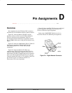
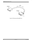
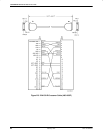
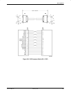
Pin Assignments
D-53550-A2-GB20-10 February 1995
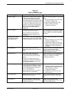
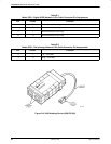
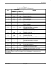
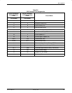
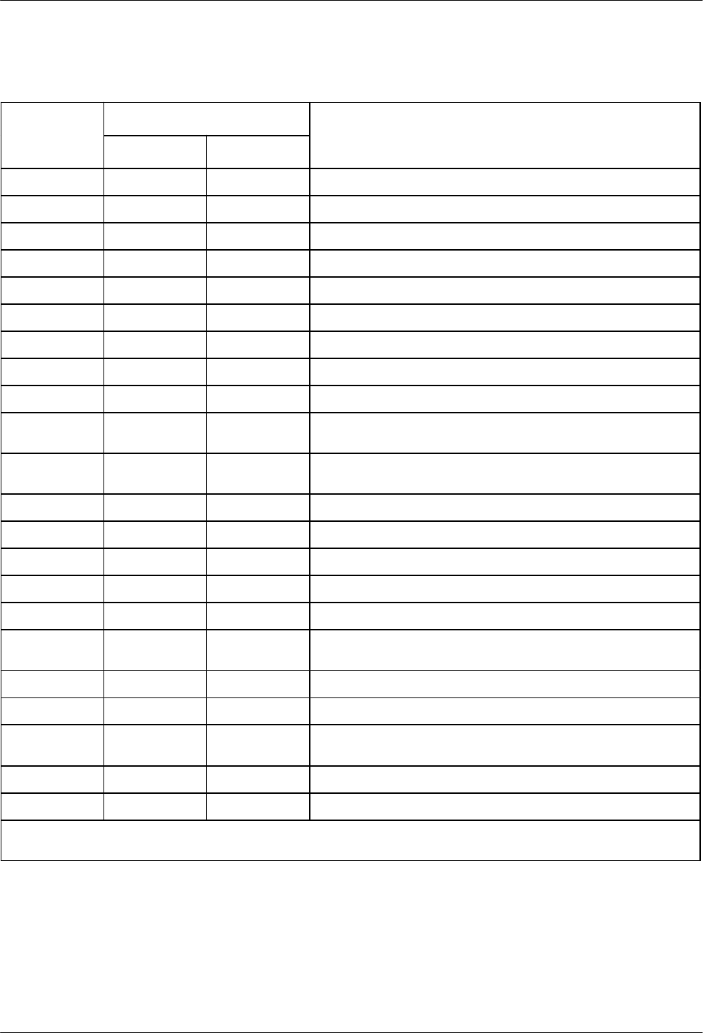
Table D-5
EIA-232/V.24 Connector Pin Assignments
Pin
Circuit Name
Function
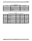
Pi
n
EIA-232
CCITT
F
unc
ti
on
2 BA 103 Transmit Data (TXD)
3 BB 104 Received Data (RXD)
4 CA 105 Request-to-Send (RTS)
5 CB 106 Clear-to-Send (CTS)
6 CC 107 Data Set Ready (DSR)
7 AB 102 Signal Ground (SG)
8 CF 109 Received Line Signal Detect (LSD)
9 — — Positive Test Voltage
10 — — Negative Test Voltage
12 CI 112 Data Signal Rate Selector I – DCE Source
(alternate external control lead I)
13
1
— — Data Signal Rate Selector II – DCE Source
(alternate external control Lead II)
14 SBA 118 Secondary Transmit Data
15 DB 114 Transmitter Signal Element Timing – DCE Source
16 SBB 119 Secondary Received Data
17 DD 115 Receiver Signal Element Timing – DCE Source
18 LL 141 Local Loopback (LL)
19
1
— — Data Signal Rate Selector II – DTE Source
(alternate external control alarm Lead II)
20 CD 108.2 Data Terminal Ready (DTR)
21 RL 140 Remote Digital Loopback (RL)
23
1
CH 111 Data Signal Rate Selector I – DTE Source
(alternate external control alarm Lead I)
24 DA 113 Transmitter Signal Element Timing – DTE Source
25 TM 142 Test Mode (TM)
1
Data Signal Rate Selector function is not available at this time. These leads can be used for the External
Lead functions.