


Warning
Please read this instruction carefully before use.
Switch off the power before wiring.
DVP04DA-H2 is an OPEN-TYPE device and therefore should be installed in an enclosure free of airborne dust,
humidity, electric shock and vibration. The enclosure should prevent non-maintenance staff from operating the
device (e.g. key or specific tools are required to open the enclosure) in case danger and damage on the device may
occur.
DO NOT connect input AC power supply to any of the I/O terminals; otherwise serious damage may occur. Check
all the wiring again before switching on the power.
DO NOT touch any terminal when the power is switched on. DO NOT touch any internal circuit in 1 minute after
the power is switched off.
Make sure the groud terminal is correctly grounded in order to prevent electromagnetic interference.
Introduction
Model Explanation & Peripherals
Thank you for choosing Delta DVP series PLC. The data in DVP04DA-H2 can be read or written
FROM/TO instructions given by the program of DVP-EH2 series MPU. The analog signal output module
receives 4 groups of 12-bit digital data from PLC MPU and converts the data into 4 points of analog
signals for output in either voltage or current.
You can select voltage or current output by wiring. Range of voltage output: 0V ~ +10V DC (resolution:
2.5mV). Range of current output: 0mA ~ 20mA (resolution: 5µA).
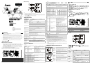
Product Profile (Indicators, Terminal Block, I/O Terminals)
Unit: mm
D - V + I +
C OM
24 V 0V
V +
I +
V +
I +
C OM
D + C OM
8
C H1 C H3 C H4R S-4 85
F G
V +
F G C OM F G
I +
C H2
1
DIN rail (35mm)
6
Terminals
2
Connection port for extension modules
7
Mounting hole
3
Model name
8
I/O terminals
4
POWER, ERROR, D/A indicator
9
Mounting port for extension modules
5
DIN rail clip
ENGLISH
External Wiring
V+
I+
COM
V+
I+
COM
24+
24-
DC/DC
+15V
-15V
AG
FG
FG
CH1
CH1
0V~+10V
*2
*3
0mA~20mA
DC24V
CH4
CH4
AC drive, recorder,
scale valve...
AC drive, recorder,
scale valve...
voltage output
shielding cable *1
shielding cable *1
current output
converter
terminal of
power module
system grounding
class 3 grounding
(100
or less)
Note:
1. When performing analog output, please isolate other power wirings.
2. If the ripples at the loaded input terminal are too significant that causes noise interference on the wiring, connect the
wiring to 0.1 ~ 0.47µF 25V capacitor.
3. Please connect the terminal on both the power modules and DVP04DA-H2 to the system earth point and ground the
system contact or connect it to the cover of power distribution cabinet.
4. DO NOT wire empty terminals
.
Specifications
Digital/Analog (4D/A)
module
Voltage output Current output
Power supply voltage 24V DC (20.4V DC ~ 28.8V DC) (-15% ~ +20%)
Analog output channel 4 channels/module
Range of analog output 0 ~ 10V 0 ~ 20mA
Range of digital data 0 ~ 4,000 0 ~ 4,000
Resolution 12 bits (1
LSB
= 2.5mV) 12 bits (1
LSB
= 5µA)
Output impedance 0.5Ω or lower
Overall accuracy
±0.5% when in full scale (25°C, 77°F)
±1% when in full scale within the range of 0 ~ 55°C, 32 ~ 131°F
Responding time 3ms × the number of channels
Max. output current 10mA (1KΩ ~ 2MΩ) -
Tolerable load impedance
- 0 ~ 500Ω
Digital data format 11 significant bits out of 16 bits are available; in 2’s complement.
Isolation
Internal circuit and analog output terminals are isolated by optical coupler.
No isolation among analog channels.
Protection
Voltage output is protected by short circuit. Short circuit lasting for too long may cause
damage on internal circuits. Current output can be open circuit.
Communication mode
ASCII/RTU mode.
(RS-485) Communication speed: 4,800/9,600/19,200/38,400/57,600/115,200 bps.
ASCII data format: 7-bit, even bit, 1 stop bit (7, E, 1).
RTU data format: 8-bit, even bit, 1 stop bit (8, E, 1).
RS-485 cannot be used when connected to PLC MPU.
When connected to
DVP-PLC MPU in series
The modules are numbered from 0 to 7 automatically by their distance from MPU. No.0 is
the closest to MPU and No.7 is the furthest. Maximum 8 modules are allowed to connect to
MPU and will not occupy any digital I/O points.
Other Specifications
Power supply
Max. rated power
consumption
24V DC (20.4V DC ~ 28.8V DC) (-15% ~ +20%), 4.5W, supplied by external power.
Environment
Operation/storage
Operation: 0°C ~ 55°C (temperature); 50 ~ 95% (humidity); pollution degree 2
Storage: -25°C ~ 70°C (temperature); 5 ~ 95% (humidity)
Vibration/shock
immunity
International standards: IEC 61131-2, IEC 68-2-6 (TEST Fc)/IEC 61131-2 & IEC 68-2-27
(TEST Ea)
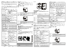
Control Registers
CR
#
RS-485
parameter
address
Latched
Register content b15
b14
b13
b12
b11
b10
b9
b8
b7
b6
b5
b4
b3
b2
b1
b0
#0
H’4032
R
Model name
Set up by the system. DVP04DA-H2 model code = H’6401.
The user can read the model name from the program and see
if the extension module exists.
Reserved CH4 CH3 CH2 CH1
#1 H’4033
R/W
Output mode setting
Output mode: Default = H’0000
Mode 0: Voltage output (0V ~ 10V)
Mode 1: Voltage output (2V ~ 10V)
Mode 2: Current output (4mA ~ 20mA)
Mode 3: Current output (0mA ~ 20mA)
CR#1: The working mode of the four channels in the analog input module. There are 4 modes for each channel which c
an
be set up separately. For example, if the user needs to set up CH1: mode 0 (b2 ~ b0 = 000); CH2: mode 1 (b5 ~ b3 = 001),
CH3: mode 2 (b8 ~ b6 = 010) and CH4: mode 3 (b11 ~ b9 = 011), CR#1 has to be set as H’
000A and the higher bits (b12 ~
b15) have to be reserved. Default value = H’0000.
#6
H’4038
R/W
CH1 output value
#7
H’4039
R/W
CH2 output value
#8
H’403A
R/W
CH3 output value
#9
H’403B
R/W
CH4 output value
Range of output value at CH1 ~ CH4: K0 ~ K4,000
Default = K0 (unit: LSB)
#18
H’4044
R/W
Adjusted OFFSET value of CH1
#19
H’4045
R/W
Adjusted OFFSET value of CH2
#20
H’4046
R/W
Adjusted OFFSET value of CH3
#21
H’4047
R/W
Adjusted OFFSET value of CH4
Range of OFFSET at CH1 ~ CH4: K-2,000 ~ K2,000
Default = K0 (unit: LSB)
#24
H’404A
R/W
Adjusted GAIN value of CH1
#25
H’404B
R/W
Adjusted GAIN value of CH2
#26
H’404C
R/W
Adjusted GAIN value of CH3
Range of GAIN at CH1 ~ CH4: K0 ~ K4,000
Default = K2,000 (unit: LSB)
CR
#
RS-485
parameter
address
Latched
Register content b15
b14
b13
b12
b11
b10
b9
b8
b7
b6
b5
b4
b3
b2
b1
b0
#27
H’404D
R/W
Adjusted GAIN value of CH4
CR#18 ~ CR#27: Please note that: GAIN value - OFFSET value = +400
LSB
~ +6,000
LSB
(voltage or current). When GAIN -
OFFSET is small (steep oblique), the resolution of output signal will be finer and variation on the digital value will be
greater. When GAIN - OFFSET is big (gradual oblique), the resolution of output signal will be rougher and variation on the
digital value will be smaller.
#30
H’4050
R Error status
Register for storing all error status.
See the table of error status for more information.
CR#30: Error status value (See the table below)
Error status Content b15 ~ b8 b7 b6 b5 b4 b3 b2 b1 b0
Abnormal power supply K1 (H’1) 0 0 0 0 0 0 0 1
Incorrect analog input value K2 (H’2) 0 0 0 0 0 0 1 0
Incorrect mode setting K4 (H’4) 0 0 0 0 0 1 0 0
OFFSET/GAIN error K8 (H’8) 0 0 0 0 1 0 0 0
Hardware malfunction K16 (H’10) 0 0 0 1 0 0 0 0
Abnormal digital range K32 (H’20) 0 0 1 0 0 0 0 0
Incorrect average times setting K64 (H’40) 0 1 0 0 0 0 0 0
Instruction error K128 (H’80)
Reserved
1 0 0 0 0 0 0 0
Note: Each error status is determined by the corresponding bit (b0 ~ b7) and there may be more than 2 errors occurring at the
same time. 0 = normal; 1 = error.
Example: Iif the digital input exceeds 4,000, error (K2) will occur. If the analog output exceeds 10V, both analog input value
error K2 and K32 will occur.
#31
H’4051
R/W
Communication address setting
For setting up RS-485 communication address.
Range: 01 ~ 254. Default = K1
#32
H’4052
R/W
Communication speed (baud
rate) setting
Default = H’0002. For setting up communication speed: 4,800
/9,600/19,200/38,400/57,600/115,200 bps.
ASCII data format: 7-bit, even bit, 1 stop bit (7, E, 1).
RTU data format: 8-bit, even bit, 1 stop bit (8, E, 1).
b0: 4,800 bps. b1: 9,600 bps (Default).
b2: 19,200 bps. b3: 38,400 bps.
b4: 57,600 bps. b5: 115,200 bps.
b6 ~ b13: Reserved.
b14: High/low bit exchange of CRC checksum (only valid in
RTU mode).
b15: Switch between ASCII/RTU mode. 0 = ASCII mode
(Default).
Reserved CH4 CH3 CH2 CH1
#33
H’4053
R/W
Return to default setting;
OFFSET/GAIN tuning
authorization
Default = H’0000. Take the setting of CH1 for example:
1. When b0 = 0, the user is allowed to tune CR#18
(OFFSET) and CR#24 (GAIN) of CH1. When b0 = 1, the
user is not allowed to tune CR#18 (OFFSET) and CR#24
(GAIN) of CH1.
2. b1 represents whether the OFFSET/GAIN tuning registers
are latched. b1 = 0 (default, latched); b1 = 1 (non-latched).
3. When b2 = 1, all settings will return to default values.
(except CR#31, CR#32)
CR#33: For authorizations on some internal functions, e.g. OFFSET/GAIN tuning. The latched function will store the
output setting in the internal memory before the power is cut off.
#34
H’4054
R
Firmware version
Displaying the current firmware version In hex; e.g. version
1.0A is indicated as H’010A.
#35 ~ #48 For system use.
Symbols:
:Latched (when written in through RS-485 communication);
: Non-latched;
R: Able to read data by FROM instruction or RS-485 communication;
W: Able to write data by TO instruction or RS-485 communication.
LSB (Least Significant Bit):
For voltage output: 1
LSB
= 10V/4,000 = 2.5mV. For current output: 1
LSB
= 20mA/4,000 = 5µA.
CR#0 ~ CR#34: The corresponding parameter addresses H’4032 ~ H’4054 are for users to read/write data by
RS-485 communication. When using RS-485, the user has to separate the module with MPU first.
a. Communication baud rate: 4,800/9,600/19,200/38,400/57,600/115,200 bps.
b. Modbus ASCII/RTU communication protocols: ASCII data format (7-bit, even bit, 1 stop bit (7, E, 1));
RTU data format (8-bit, even bit, 1 stop bit (8, E, 1)).
c. Function: H’03 (read register data); H’06 (write 1 word datum to register); H’10 (write many word data to
register).
d. Latched CR should be written by RS-485 communication to stay latched. CR will not be latched if written
by MPU through TO/DTO instruction.
Adjusting D/A Conversion Curve
Voltage output mode
CR#1 mode 0 GAIN = 5V (2,000
LSB
). OFFSET = 0V (0
LSB
).
CR#1 mode 1 GAIN = 6V (2,400
LSB
). OFFSET = 2V (800
LSB
).
GAIN
The voltage output value when the digital input value = K2,000.
Range: 0
LSB
~ +4,000
LSB
.
OFFSET
The voltage output value when the digital input value = K0.
Range: -2,000
LSB
~ +2,000
LSB
.
+2,000
+4,000
2V
5V
6V
10V
OFFSET
GAIN
V
o
l
t
a
g
e
o
u
t
p
u
t
Digital input
Mode 1
Mode 0
GAIN - OFFSET
Range: +400
LSB
~ +6,000
LSB
.
Current output mode
CR#1 mode 2 GAIN = 12mA (2,400
LSB
). OFFSET = 4mA (800
LSB
).
CR#1 mode 3 GAIN = 10mA (2,000
LSB
). OFFSET = 0mA (0
LSB
).
GAIN
The current output value when the digital input value = K2,000.
Range: 0
LSB
~ +4,000
LSB
.
OFFSET
The current output value when the digital input value = K0.
Range: -2,000
LSB
~ +2,000
LSB
.
0
+2,000
+4,000
20mA
OFFSET
GAIN
12mA
10mA
4mA
C
u
r
r
e
n
t
o
u
t
p
u
t
Digital input
Mode 2
Mode 3
GAIN - OFFSET
Range: +400
LSB
~ +6,000
LSB
.
(OPEN TYPE) /
DVP DVP04DA-H2 DVP-EH2
FROM/TO DVP04DA-H2 PLC 4
12 4
0V ~ +10V DC 2.5mV
0mA ~ 20mA 5µA
mm
D - V + I +
C OM
24V 0V
V +
I +
V +
I +
C OM
D + C OM
8
C H1 C H3 CH4R S-48 5
F G
V +
F G C OM F G
I +
C H2
1
DIN (35mm)
6
2
/
7
3
8
4
9
/
5
DIN
V+
I+
COM
V+
I+
COM
24+
24-
DC/DC
+15V
-15V
AG
FG
FG
CH1
CH1
*1
0V~+10V
*2
*3
*1
0mA~20mA
DC24V
CH4
100
CH4
1
2 0.1 ~ 0.47µF 25V
3 DVP04DA-H2
(4D/A)
24V DC (20.4V DC ~ 28.8V DC) (-15% ~ +20%)
4 /
0 ~ 10V 0 ~ 20mA
0 ~ 4,000 0 ~ 4,000
12 bits (1
LSB
= 2.5mV) 12 bits (1
LSB
= 5µA)
0.5Ω
±0.5% 25°C, 77°F ±1% 0 ~ 55°C, 32 ~ 131°F
3ms ×
10mA (1KΩ ~ 2MΩ)
0 ~ 500Ω
16 11 bits
(RS-485)
ASCII/RTU 4,800/9,600/19,200/38,400/57,600/115,200 bps ASCII
7 bits 1 stop bit (7, E, 1) RTU 8 bits
1 stop bit (8, E, 1) PLC RS-485