


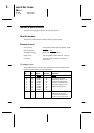
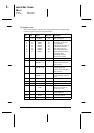

Pin assignments
The parallel interface connector pin assignments and a description of the
interface signals are shown in the table below.
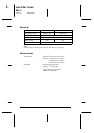
Signal
Pin
Return
Pin Signal Direction Description
1 19 HostClk IN Host clock signal.
2
3
4
5
6
7
8
9
20
21
22
23
24
25
26
27
DATA 0
DATA 1
DATA 2
DATA 3
DATA 4
DATA 5
DATA 6
DATA 7
IN
IN
IN
IN
IN
IN
IN
IN
These signals represent
information in bits 0 to 7
of parallel data
respectively. Each signal
is at HIGH level when
data is logical 1 and
LOW when it is logical 0.
These signals are used to
transfer the 1284
extensibility request
values to the printer.
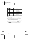
10 28 PtrClk OUT Printer clock signal.
11 29 PtrBusy/
DataBit - 3, 7
OUT Printer busy signal and
reverse channel transfer
data bit 3 or 7.
12 28 AckDataReq/
DataBit - 2, 6
OUT Acknowledge data
request signal and
reverse channel transfer
data bit 2 or 6.
13 28 Xflag/
DataBit - 1, 5
OUT X-flag signal and reverse
channel transfer data bit
1 or 5
14 30 HostBusy IN Host busy signal.
15 - NC - Not used
16 - GND - Logic ground level
17 - CHASSIS
GND
- Printer’s chassis ground,
which is connected to
the logic ground.
18 - Logic H OUT Pulled up to +5 V through
3.9 kΩ resistance
19-30 - GND - Logic ground level
31 30
INIT IN Not used.
L
Loire2 Ref. Guide
Rev.c
A5 size Appendix C
11-11-96 DR, pass 0
C-18
Specifications