12 EPSON S1C88650 TECHNICAL MANUAL
3 CPU AND BUS CONFIGURATION
3.6.2 Address bus
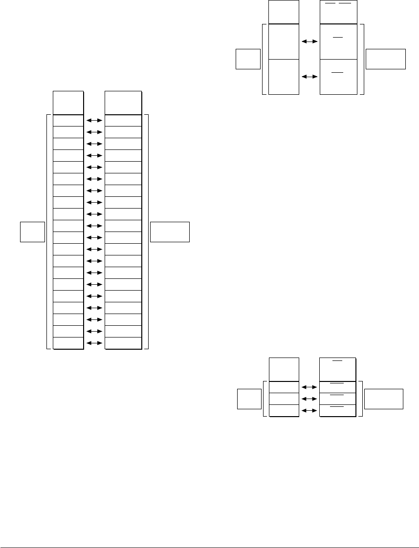
The S1C88650 possesses a 20-bit external address
bus A0–A19. The terminals and output circuits of
address bus A0–A19 are shared with output ports
R00–R07 (=A0–A7), R10–R17 (=A8–A15) and R20–
R23 (=A16–A19), switching between these functions
being determined by the bus mode setting.
In the single chip mode, the 20-bit terminals are all
set as output ports R00–R07, R10–R17 and R20–R23.
In the expansion mode, all of the 20-bit terminals
are set as the address bus (A0–A19).
When set as an address bus, the data register and
high impedance control register of each output port
are detached from the output circuit and used as a
general purpose data register with read/write
capabilities.
Output
port
Address
bus
R00
R01
R02
R03
R04
R05
R06
R07
R10
R11
R12
R13
R14
R15
R16
R17
R20
R21
R22
R23
A0
A1
A2
A3
A4
A5
A6
A7
A8
A9
A10
A11
A12
A13
A14
A15
A16
A17
A18
A19
Bus modeBus mode
Single
chip
Expansion
Fig. 3.6.2.1 Correspondence between address bus
and output ports
_____ ______
3.6.3 Read (RD)/write (WR) signals
The output terminals and output circuits for the
____ _____
read (RD)/write (WR) signals directed to external
devices are shared respectively with output ports
R24 and R25, switching between these functions
being determined by the bus mode setting.
In the single chip mode, both of these terminals are
set as output port terminals and in the expansion
____ _____
mode, they are set as read (RD)/write (WR) signal
output terminals.
____ _____
When set as read (RD)/write (WR) signal output
terminal, the data register and high impedance
control register for each output port (R24, R25) are
detached from the output circuit and is usable as a
general purpose data register with read/write
capabilities.
See Section 3.6.5, "WAIT control", for the output
timing of the signal.
Output
port
RD/WR
signal
R24
R25
RD
WR
Bus mode
Bus mode
Single
chip
Expansion
____
Fig. 3.6.3.1 Correspondence between read (RD)/
_____
write (WR) signal and output ports
_____
3.6.4 Chip enable (CE) signal
The S1C88650 is equipped with address decoders
____
which can output three different chip enable (CE)
signals.
Consequently, three devices equipped with a chip
_____ _____
enable (CE) or chip select (CS) terminal can be
directly connected without setting the address
decoder to an external device.
_____ _____
The three chip enable (CE0–CE2) signal output
terminals and output circuits are shared with
output ports R30–R32 and in the expansion mode,
____
either the chip enable (CE) output or general output
can be selected in software for each of the three bits.
____
When set for chip enable (CE) output, the data
register and high impedance control register for
each output port are detached from the output
circuit and is usable as general purpose data
register with read/write capabilities.
In the single chip mode, these terminals are set as
output ports R30–R32.
Output
port
CE
signal
R30
R31
R32
CE0
CE1
CE2
Bus mode
B
us mode
Single
chip
Expansion
____
Fig. 3.6.4.1 Correspondence between CE signals
and output ports
Table 3.6.4.1 shows the address ranges which are
____
assigned to the chip enable (CE) signal in the
expansion mode.


