S1C88650 TECHNICAL MANUAL EPSON 69
5 PERIPHERAL CIRCUITS AND THEIR OPERATION (Serial Interface)
5.8.7 Operation of asynchronous transfer
Asynchronous transfer is a mode that transfers by
adding a start bit and a stop bit to the front and the
back of each piece of serial converted data. In this
mode, there is no need to use a clock that is fully
synchronized clock on the transmit side and the
receive side, but rather transmission is done while
adopting the synchronization at the start/stop bits
that have attached before and after each piece of
data. The RS-232C interface functions can be easily
realized by selecting this transfer mode.
This interface has separate transmit and receive
shift registers and is designed to permit full duplex
transmission to be done simultaneously for trans-
mitting and receiving.
For transfer data in the asynchronous 7-bit mode,
either 7 bits data (no parity) or 7 bits data + parity
bit can be selected. In the asynchronous 8-bit mode,
either 8 bits data (no parity) or 8 bits data + parity
bit can be selected.
Parity can be even or odd, and parity checking of
received data and adding a party bit to transmitting
data will be done automatically. Thereafter, it is not
necessary to be conscious of parity itself in the
program.
The start bit length is fixed at 1 bit. For the stop bit
length, either 1 bit or 2 bits can be selected using
the stop bit select register STPB. Whether data is
transmitted/received from LSB (bit 0) or MSB (bit
7) it can be switched using the data input/output
permutation select register SDP.
■ Initialization of serial interface
The below initialization must be done in cases of
asynchronous system transfer.
(1) Setting of transmitting/receiving disable
To set the serial interface into a status in which
both transmitting and receiving are disabled, "0"
must be written to both the transmit enable
register TXEN and the receive enable register
RXEN. Fix these two registers to a disable status
until data transfer actually begins.
(2) Port selection
Because serial interface input/output terminals
SIN and SOUT are set as I/O port terminals P10
and P11 at initial reset, "1" must be written to
the serial interface enable register ESIF in order
to set these terminals for serial interface use.
_________ _________
SCLK and SRDY terminals set in the clock
synchronous mode are not used in the asynchro-
nous mode. These terminals function as I/O
port terminals P12 and P13.
(3) Setting of transfer mode
Select the asynchronous mode by writing the
data as indicated below to the two bits of the
mode selection registers SMD0 and SMD1.
7-bit mode: SMD0 = "0", SMD1 = "1"
8-bit mode: SMD0 = "1", SMD1 = "1"
(4) Parity bit selection
When checking and adding parity bits, write "1"
into the parity enable register EPR to set to "with
parity check". As a result of this setting, in the
asynchronous 7-bit mode, it has a 7 bits data +
parity bit configuration and in the asynchronous
8-bit mode it has an 8 bits data + parity bit
configuration.In this case, parity checking for
receiving and adding a party bit for transmitting
is done automatically in hardware. Moreover,
when "with parity check" has been selected,
"odd" or "even" parity must be further selected in
the parity mode selection register PMD.
When "0" is written to the PMD register to select
"without parity check" in the asynchronous 7-bit
mode, data configuration is set to 7 bits data (no
parity) and in the asynchronous 8-bit mode (no
parity) it is set to 8 bits data (no parity) and parity
checking and parity bit adding will not be done.
(5) Clock source selection
Select the clock source by writing data to the
two bits of the clock source selection registers
SCS0 and SCS1. (See Table 5.8.4.1.)
Since all the registers mentioned in (2)–(5) are
assigned to the same address, it's possible to set
them all with one instruction.
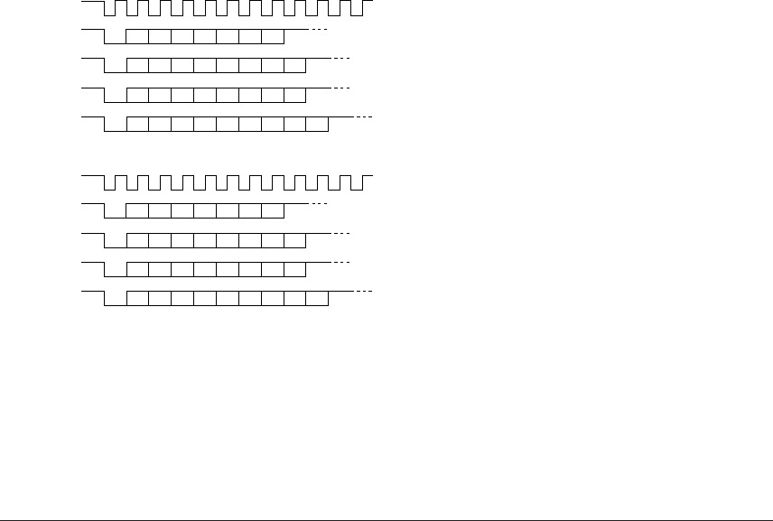
Sampling
clock
8bit data D7
D6 D5 D4 D3 D2 D1 D0s1 s2
7bit data
+parity
D6
D5 D4 D3 D2 D1 D0 ps1 s2
8bit data
+parity
D7 D6 D5 D4 D3 D2 D1 D0s1 p s2
s1
s2
p
: Start bit (Low level, 1 bit)
: Stop bit (High level, 1 bit or 2 bits)
: Parity bit
7bit data D6
D5 D4 D3 D2 D1 D0s1 s2
Sampling
clock
LSB first
MSB first
8bit data D0 D1 D2 D3 D4 D5 D6 D7s1 s2
7bit data
+parity
D0
D1 D2 D3 D4 D5 D6 ps1 s2
8bit data
+parity
D0
D1 D2 D3 D4 D5 D6 D7s1 p s2
7bit data D0
D1 D2 D3 D4 D5 D6s1 s2
Fig. 5.8.7.1 Transfer data configuration
for asynchronous system
Here following, we will explain the control se-
quence and operation for initialization and trans-
mitting /receiving in case of asynchronous data
transfer. See "5.8.8 Interrupt function" for the serial
interface interrupts.


