5700A/5720A Series II Calibrator
Service Manual
2-68
2-109. Negative Offset Circuit
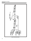
This circuit creates a constant offset voltage of approximately -127 mV at the filter
input. Thus, for a DAC output voltage of 0V, the first channel count must be
approximately 400 to offset this negative voltage. This guarantees a minimum duty cycle
pulse width of approximately 50 us.
This minimum duty cycle is necessary to overcome the offset of the output stage and to
allow the reference voltage to settle out after being switched into the filter input. Op amp
U2A and two 20 kΩ resistors in HR6 form an amplifier with an inverting gain of 1. This
amplifier input is the 13V reference which produces -13V at its output. This -13V is
divided by resistors in the HR5 assembly to create the -127 mV on the filter input.
2-110. DAC Output Switching
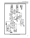
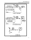
The floating outputs of the DAC are switched with latching-type relays K1, K2, K3, K4,
and K8.
Relays K1 and K2 determine the polarity of the DAC. In the reset position, the DAC
output is positive. In the set position, output is negative. Relay K1 also generates DAC
LO DIAG and DAC HI DIAG which are used by the adc circuit during DAC diagnostics.
Relays K3 and K4 switch the DAC to various assemblies. In the reset position, the DAC
is available to all assemblies except the oscillator. Relays K3 and K4 are set during
operation in the ac function so the DAC output is connected to the DAC/OSC lines
which run only to the Oscillator assembly. Also during operation in the ac function,
control line DAC OUT SEL turns on FET Q25, via FET Q26, to connect SCOM to
RCOM.
Relay K8, when in the set position, allows the DAC to be sensed right on the output of
the DAC assembly.
2-111. DAC Buffered Reference Sip
The DAC Buffered Reference SIP assembly (A11A2) has two main functions. First, it
buffers the 6.5V and 13V references so they can be used by other assemblies.
The 6.5V reference, REF6, is buffered by op amps U1A and U2A which creates BRF6
and its sense line BSRF6. The 13V reference, REF13 FILT, is buffered by op amps U1B
and U2B which creates BRF13 and its sense line BSRF13. These are routed to other
assemblies in the calibrator for use during calibrator calibration.
Second, it allows the reference voltages, or the buffered reference voltages, to be
switched to the REFCAL line, which is connected to the inverting input of the adc
amplifier by K5 during calibration of the DAC assembly.
Control line REF6 SEL and FETs Q1 and Q2 connect the 6.5V reference REF6 to
REFCAL.
Control line BSRF6 SEL and FETs Q5-Q7 tie BRF6 and BSRF6 together and connect
them to REFCAL.
Control line REF13 SEL and FETs Q8 and Q9 connect the 13V reference REF13 to
REFCAL.
Control line BSRF13 SEL and FETs Q12-Q14 tie BRF13 and BSRF13 together and
connect them to REFCAL.
ADC COM can also be connected to REFCAL by FET Q15 and control line ADC COM
SEL.


