5700A/5720A Series II Calibrator
Service Manual
2-70
2-115. ADC Circuit
The adc (analog-to-digital converter) is shown on sheet 5 of the DAC schematic.
Most of the adc is contained on one chip (U25) which uses the Fluke-patented
recirculating remainder technique.
The adc has rms noise of approximately 20 µV between readings. This is reduced by a
factor of 5 by averaging the readings. The adc measures input voltages between -1.8V
and +1.8V.
Hardware for the adc has four major sections external to adc IC U25. These sections are:
• ADC reference voltage
• ADC dac
• ADC comparator/amplifier
• Timing/data control circuitry.
The adc reference voltage circuit is made up of zener diodes VR29, VR30, and resistors
R91-R93, which generate a 6.4V reference. This -6.4V is inverted by U27B to create the
+6.4V reference and is also buffered by U27A and connected to U25. A reference
common point for the adc reference is made by buffering ADC COM with op amps
U20B and U26A, resulting in an isolated ADC COM. Buffering allows the common
point to be referenced to ADC COM, yet current from R85, C89, C90, R93, VR29, and
VR30 to return to SCOM through the output of the buffer instead of through ADC COM.
The adc dac contains the dac amplifier, U28B, and a binary ladder network consisting of
resistors in Z10. Digitally controlled analog bit switches are contained in U25. The bit
switches determine the output voltage of U28B by control of the binary ladder network.
The output voltage of U28B can be varied from -1.95V to 1.95V.
The adc comparator/amplifier contains op amp U29, two remainder storage capacitors
(C89 and C90), an autozero storage capacitor (C95), and several digitally-controlled
analog switches in U25.
The supplies for U29 are bootstrapped off its input voltage. This circuitry includes
U28A, VR31-VR34, R95-R100, Q56, Q57, and C97.
The timing/data control circuit is the digital portion of U25. This internal circuitry
controls the adc by manipulating the switches in the adc comparator/amplifier and the bit
switches in the adc dac.
An adc conversion cycle is triggered by the falling edge of control line ADC TRIGGER
from the digital control circuit. Once triggered, the adc, under control by U25, generates
five 6-bit nibbles without any further interaction.
Once the adc is triggered, it goes through five measurement cycles. Each cycle is made
up of three functions, an autozero function, a compare function and a remainder store
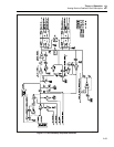
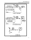
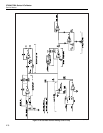
function. Figure 2-18 illustrates these three functions.
Before the adc is triggered, it stays in the autozero function. In this function, the adc dac
is set to 0V with some offset error. Through U25, pin 3 of U29 is connected to ADC
COM and pins 2 and 6 are connected together. In this function, the offset of the adc dac
is stored on C95.
In the compare function, U29 compares the adc dac with the adc input (during the first
pass) or the stored remainder (C89 or C90) during the remaining four passes. The
voltage to be measured is switched into pin 3. The adc dac is connected to pin 2 and
adjusted according to the polarity output of U29 resolving the voltage on pin 3. During
this function the six bits of one nibble are determined.


