5700A/5720A Series II Calibrator
Service Manual
2-128
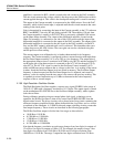
amplifier is connected to RCL, which is routed to the adc circuit on the DAC assembly.
The adc circuit measures the voltage, which is the drop across the 100Ω resistor with no
current applied through it. This value is the checkpoint reading and is stored in memory.
The output of the Current assembly is reconnected to the 100Ω resistor. Next, the DAC
assembly, which is the Current input, is adjusted until the adc circuit measures the same
reading as the check point.
Gain is determined by connecting the input of the Current assembly to the 13V reference
BRF13 and BSRF13 via relay K1 and analog switch U5B. The resulting 130 mA from
the Current assembly is routed via INT OUT HI to a previously calibrated 10W resistor
on the Ohms Main assembly. The +input of the differential amplifier, located on the
Ohms Cal assembly, is connected to one side of this 10W resistor and the -input of the
differential amplifier is connected to the output of the DAC assembly. The output of the
differential amplifier is connected to the adc circuit in the DAC assembly via the RCL
line, and the DAC output is adjusted until a null is achieved. This determines the exact
voltage drop across the 10W resistor. The exact gain can now be calculated using this
and the previous offset reading.
The current output, now calibrated at dc, is further characterized for its frequency
response. The Current assembly is configured to the ac current function with input from
the Oscillator Output assembly (A13) set to 20V at a low frequency. The output side of
the appropriate shunt resistor is connected to SCOM by relay K17B, and the resulting 2V
on the input side of the shunt resistor is connected to the AC CAL line through U22 by
relay K17A. The AC CAL signal is routed to the Oscillator Control assembly (A12)
where a 400Ω rms sensor measures the ac voltage on this line. A dc reading of the sensor
is taken. It and the Oscillator Output level are stored in memory. The Oscillator Output
frequency is then increased and the Oscillator Output level is adjusted, and stored in
memory, so the dc reading from the rms sensor is the same as the previous reading. This
is repeated at various frequencies up to 10 kHz to characterize the entire frequency
response of the ac current output.
2-199. High-Resolution Oscillator Section
The High-Resolution Oscillator supplies a square-wave signal (HI-RES) in the range of
10 Hz to 1.2 MHz with a frequency resolution of 4 1/2 digits. The output signal is routed
on the motherboard P LOCK HI line to the Oscillator Output assembly, where it phase-
locks the oscillator.
During calibrator operation using an external phase-lock signal, or during a non-ac
operation, the Hi-Res Oscillator is shut off by control line HI RES ON/OFF from the
digital control circuit. The hi-res circuitry uses a phase-locked loop circuit containing the
reference frequency amplifier/divider, phase detector/divider, loop filter, and vco circuit
as outlined on the schematic. A 5-500k divider and output switching circuitry creates the
final output frequency. These circuits are described in the following paragraphs.
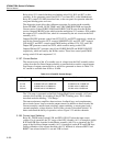
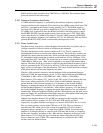
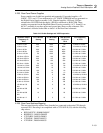
The Hi-Res Oscillator output is divided into five ranges as shown below:
• 10.00 Hz to 119.99 Hz
• 0.1200 kHz to 1.1999 kHz
• 1.200 kHz to 11.999 kHz
• 12.00 kHz to 119.99 kHz
• 0.1200 MHz to 1.1999 MHz
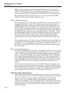
Note that the frequency resolution on each range changes from four digits for outputs of
12 to 99 to five digits for outputs of 100 to 119. For example, the output of range 1 has
four digits of resolution from 10.00 Hz to 99.99 Hz and five digits resolution from
100.00 Hz to 119.99 Hz. The range 2 output has four digits resolution from 120 Hz to


