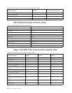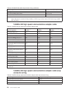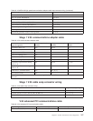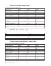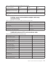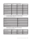
Table 74. V.35/High speed communications adapter cable (continued)
Signal designation
Interchange circuit
number
Adapter connector pin
number
DCE connector pin
number
Data terminal ready 108 36, 35 H
Transmitter signal element timing
(DTE) A, B
113 10, 27 U, W
Ring Indicate (RI) A, B 125 11, 28 J
Note: Cable ID 1, 0 is connected to common return pin 7 only at the DTE connector end and is not connected at the
DCE end.
V.35/High speed communications adapter cable wrap
connector wiring
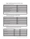
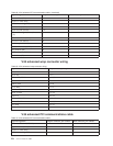
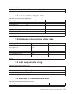
Table 75. V.35/High speed communications adapter cable wrap connector wiring
Signal designation Wrap connector pin to pin
Transmit data A to receive data A P to R
Transmit data B to receive data B S to T
RTS to CTS, RI C to (D,J)
DTR to DSR, RLSD H to (E,F)
TSET A(DTR) to TSET A(DCE), RSET A U to (V,Y)
TSET B(DTE) to TSET B(DCE), RSET B W to (X,AA)
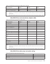
V.36/RS-449 advanced PCI communications cable
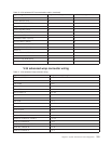
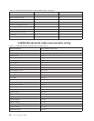
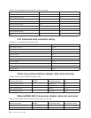
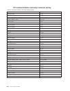
Table 76. V.36/RS-449 advanced PCI communications cable
Signal designation Adapter connector pin number DCE connector pin number
Transmitted data A (TD-A) 13 4
Transmitter clock A (TCLK-A) 29 5
Received data A (RD-A) 6 6
Request to send A (RTS-A) 2 7
Receiver clock A (RCLK-A) 26 8
Ready for sending A (CTS) 33 9
Local Loop Back (LLB) 21 10
Data set ready A (DSR-A) 15 11
Data terminal ready A (DTR-A) 4 12
Carrier detector A (DC-A) 20 13
23 14
Ring Indicate (RI) 16 15
DTECK A 36 17
Test Indicate (TI) 17 18
Signal Ground (SGND) 7,9,10,27 19
RC Ground (SC-GND) 34 20
Transmitted data B (TD-B) 12 22
Chapter 9. System Architecture and Configuration 261


