DS33R11 Ethernet Mapper with Integrated T1/E1/J1 Transceiver
208 of 344
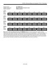
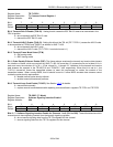
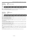
Register Name:
TR.T1CCR1
Register Description:
T1 Common Control Register 1
Register Address:
07h
Bit # 7 6 5 4 3 2 1 0
Name — — — TRAI-CI TAIS-CI TFM PDE TLOOP
Default 0 0 0 0 0 0 0 0
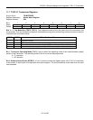
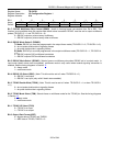
Bit 4: Transmit RAI-CI Enable (TRAI-CI). Setting this bit causes the ESF RAI-CI code to be transmitted in the
FDL bit position.
0 = do not transmit the ESF RAI-CI code
1 = transmit the ESF RAI-CI code
Bit 3: Transmit AIS-CI Enable (TAIS-CI). Setting this bit and the TBL bit (TR.T1TCR1.1) causes the AIS-CI code
to be transmitted at TPOSO and TNEGO, as defined in ANSI T1.403.
0 = do not transmit the AIS-CI code
1 = transmit the AIS-CI code (TR.T1TCR1.1 must also be set = 1)
Bit 2: Transmit Frame Mode Select (TFM)
0 = D4 framing mode
1 = ESF framing mode
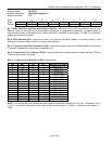
Bit 1: Pulse Density Enforcer Enable (PDE). The framer always examines the transmit and receive data streams
for violations of these, which are required by ANSI T1.403: No more than 15 consecutive 0s and at least N 1s in
each and every time window of 8 x (N + 1) bits, where N = 1 through 23. Violations for the transmit and receive
data streams are reported in the TR.INFO1.6 and TR.INFO1.7 bits, respectively. When this bit is set to 1, the
T1/E1/J1 transceiver forces the transmitted stream to meet this requirement no matter the content of the
transmitted stream. When running B8ZS, this bit should be set to 0 since B8ZS encoded data streams cannot
violate the pulse density requirements.
0 = disable transmit pulse density enforcer
1 = enable transmit pulse density enforcer
Bit 0: Transmit Loop-Code Enable (TLOOP). See Section
10.19 for details.
0 = transmit data normally
1 = replace normal transmitted data with repeating code as defined in registers TR.TCD1 and TR.TCD2
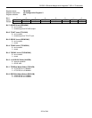
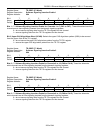
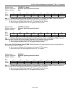
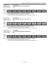
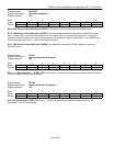
Register Name:
TR.SSIE1 (T1 Mode)
Register Description:
Software Signaling Insertion Enable 1
Register Address:
08h
Bit # 7 6 5 4 3 2 1 0
Name CH8 CH7 CH6 CH5 CH4 CH3 CH2 CH1
Default 0 0 0 0 0 0 0 0
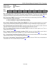
Bits 0 – 7: Software Signaling Insertion Enable for Channels 1 to 8 (CH1 to CH8). These bits determine which
channels are to have signaling inserted from the transmit signaling registers.
0 = do not source signaling data from the TR.TSx registers for this channel
1 = source signaling data from the TR.TSx registers for this channel


