7.4 BADR2
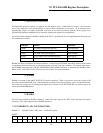
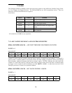
The I/O Region defined by BADR2 contains the ADC Data register and the ADC FIFO clear
register.
7.4.1 ADC DATA REGISTER
BADR2 + 0
ADC Data register.
WRITE
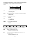
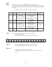
Writing to this register is only valid for SW initiated conversions. The ADC Pacer source must
be set to 00 via the ADPS[1:0] bits. A null write to BADR2 + 0 will begin a single conversion.
Conversion status may be determined in two ways. The
EOC
bit in BADR1 + 0 may be polled
until true or
ADNEI
(the AD FIFO not-empty interrupt) may be used to signal that the ADC conversion is complete
and the data word is present in the FIFO.
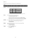
READ
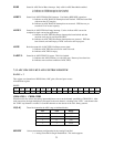
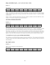
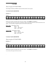
AD0AD1AD2AD3AD4AD5AD6AD7AD8AD9AD10AD110000
0123456789101112131415
MSB LSB
AD[11:0]
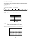
This register contains the current ADC data word. Data format is dependent upon
offset mode:
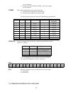
Bipolar Mode
:
Offset Binary Coding
000 h = -FS
7FFh = Mid-scale
(0V)
FFFh = +FS - 1LSB
Unipolar
Mode
:
Straight Binary Coding
000 h = -FS (0V)
7FFh = Mid-scale (+FS/2)
FFFh = +FS - 1LSB
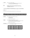
7.4.2 ADC FIFO CLEAR REGISTER
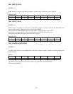
BADR2 + 2
ADC FIFO Clear register. A Write-only register. A write to this address location clears
the ADC FIFO. Data is don't care. The ADC FIFO should be cleared before all new
ADC operations.
27


