


Transistors
1
Publication date: May 2007 SJC00388AED
This product complies with the RoHS Directive (EU 2002/95/EC).
2SB1463G
Silicon PNP epitaxial planar type
For high breakdown voltage low-noise amplification
Complementary to 2SC2440G
■ Features
• High collector-emitter voltage (Base open) V
CEO
• Low noise voltage NV
• SS-Mini type package, allowing downsizing of the equipment and
automatic insertion through the tape packing.
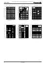
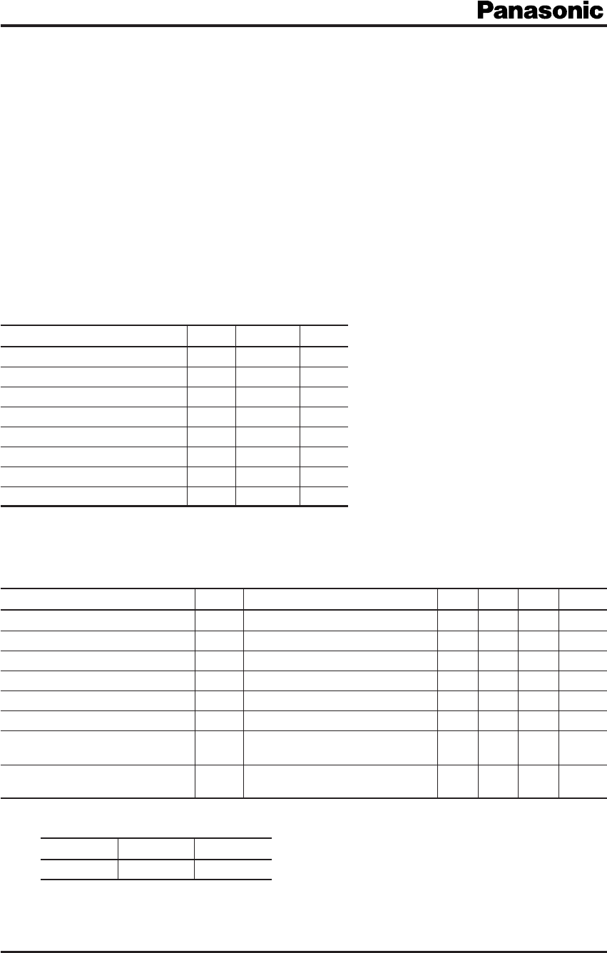
■ Absolute Maximum Ratings T
a
= 25°C
Parameter Symbol Rating Unit
Collector-base voltage (Emitter open) V
CBO
−150 V
Collector-emitter voltage (Base open) V
CEO
−150 V
Emitter-base voltage (Collector open) V
EBO
−5V
Collector current I
C
−50 mA
Peak collector current I
CP
−100 mA
Collector power dissipation P
C
125 mW
Junction temperature T
j
125 °C
Storage temperature T
stg
−55 to +125 °C
■ Electrical Characteristics T
a
= 25°C ± 3°C
Note) 1. Measuring methods are based on JAPANESE INDUSTRIAL STANDARD JIS C 7030 measuring methods for transistors.
2.
*
: Rank classification
Parameter Symbol Conditions Min Typ Max Unit
Collector-emitter voltage (Base open) V
CEO
I
C
= −100 µA, I
B
= 0 −150 V
Emitter-base voltage (Collector open) V
EBO
I
E
= −10 µA, I
C
= 0 −5V
Collector-base cutoff current (Emitter open)
I
CBO
V
CB
= −100 V, I
E
= 0 −1 µA
Forward current transfer ratio
*
h
FE
V
CE
= −5 V, I
C
= −10 mA 130 330
Collector-emitter saturation voltage V
CE(sat)
I
C
= −30 mA, I
B
= −3 mA −1V
Transition frequency f
T
V
CB
= −10 V, I
E
= 10 mA, f = 200 MHz 200 MHz
Collector output capacitance C
ob
V
CB
= −10 V, I
E
= 0, f = 1 MHz 4 pF
(Common base, input open circuited)
Noise voltage NV V
CE
= −10 V, I
C
= −1 mA, G
V
= 80 dB 150 mV
R
g
= 100 kΩ, Function = FLAT
Rank R S
h
FE
130 to 220 185 to 330
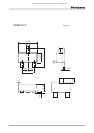
■ Package
• Code
SSMini3-F3
• Marking Symbol: I
• Pin Name
1.Base
2.Emitter
3.Collector