


Transistors
1
Publication date: March 2003 SJC00128BED
2SC3312
Silicon NPN epitaxial planar type
For low-frequency and low-noise amplification
Complementary to 2SA1310
■ Features
• Optimum for high-density mounting
• Allowing supply with the radial taping
• Low noise voltage NV
■ Absolute Maximum Ratings T
a
= 25°C
Parameter Symbol Rating Unit
Collector-base voltage (Emitter open) V
CBO
60 V
Collector-emitter voltage (Base open) V
CEO
55 V
Emitter-base voltage (Collector open) V
EBO
7V
Collector current I
C
100 mA
Peak collector current I
CP
200 mA
Collector power dissipation P
C
300 mW
Junction temperature T
j
150 °C
Storage temperature T
stg
−55 to +150 °C
Parameter Symbol Conditions Min Typ Max Unit
Collector-base voltage (Emitter open) V
CBO
I
C
= 10 µA, I
E
= 060V
Collector-emitter voltage (Base open) V
CEO
I
C
= 2 mA, I
B
= 055V
Emitter-base voltage (Collector open) V
EBO
I
E
= 10 µA, I
C
= 07V
Base-emitter voltage V
BE
V
CE
= 1 V, I
C
= 30 mA 1 V
Collector-base cutoff current (Emitter open)
I
CBO
V
CB
= 20 V, I
E
= 0 0.1 µA
Collector-emitter cutoff current (Base open)
I
CEO
V
CE
= 20 V, I
B
= 01µA
Forward current transfer ratio
*
h
FE
V
CE
= 5 V, I
C
= 2 mA 180 700
Collector-emitter saturation voltage V
CE(sat)
I
C
= 100 mA, I
B
= 10 mA 1 V
Transition frequency f
T
V
CB
= 5 V, I
E
= −2 mA, f = 200 MHz 200 MHz
Noise voltage NV V
CE
= 10 V, I
C
= 1 mA, G
V
= 80 dB 150 mV
R
g
= 100 kΩ, Function = FLAT
■ Electrical Characteristics T
a
= 25°C ± 3°C
Unit: mm
Note) 1. Measuring methods are based on JAPANESE INDUSTRIAL STANDARD JIS C 7030 measuring methods for transistors.
2.
*
: Rank classification
Rank R S T
h
FE
180 to 360 260 to 520 360 to 700
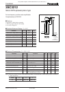
4.0±0.2
0.75 max.
2.0
±0.2
0.45
(2.5) (2.5)
0.7
±0.1
231
+0.20
–0.10
0.45
+0.20
–0.10
7.6
3.0
±0.2
(0.8)(0.8)
15.6
±0.5
1: Emitter
2: Collector
3: Base
NS-B1 Package
This product complies with the RoHS Directive (EU 2002/95/EC).