


1
Transistors
Publication date: April 2007 SJC00358AED
2SC3931G
Silicon NPN epitaxial planar type
For high-frequency amplification
■ Features
• Optimum for RF amplification of FM/AM radios
• High transition frequency f
T
• S-Mini type package, allowing downsizing of the equipment and
automatic insertion through the tape packing
■ Absolute Maximum Ratings T
a
= 25°C
Parameter Symbol Rating Unit
Collector-base voltage (Emitter open) V
CBO
30 V
Collector-emitter voltage (Base open) V
CEO
20 V
Emitter-base voltage (Collector open) V
EBO
3V
Collector current I
C
15 mA
Collector power dissipation P
C
150 mW
Junction temperature T
j
150 °C
Storage temperature T
stg
−55 to +150 °C
Parameter Symbol Conditions Min Typ Max Unit
Collector-base voltage (Emitter open) V
CBO
I
C
= 10 µA, I
E
= 030V
Emitter-base voltage (Collector open) V
EBO
I
E
= 10 µA, I
C
= 03V
Base-emitter voltage V
BE
V
CB
= 6 V, I
E
= −1 mA 720 mV
Forward current transfer ratio
*
h
FE
V
CB
= 6 V, I
E
= −1 mA 65 260
Transition frequency f
T
V
CB
= 6 V, I
E
= −1 mA, f = 200 MHz 450 650 MHz
Common-emitter reverse transfer C
re
V
CB
= 6 V, I
E
= −1 mA, f = 10.7 MHz 0.8 1.0 pF
capacitance
Power gain G
P
V
CB
= 6 V, I
E
= −1 mA, f = 100 MHz 24 dB
Noise figure NF V
CB
= 6 V, I
E
= −1 mA, f = 100 MHz 3.3 dB
■ Electrical Characteristics T
a
= 25°C ± 3°C
Note) 1. Measuring methods are based on JAPANESE INDUSTRIAL STANDARD JIS C 7030 measuring methods for transistors.
2.
*
: Rank classification
Rank C D
h
FE
65 to 160 100 to 260
This product complies with the RoHS Directive (EU 2002/95/EC).
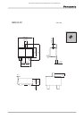
■ Package
• Code
SMini3-F2
• Marking Symbol: U
• Pin Name
1.Base
2.Emitter
3.Collector