


Transistors
1
Publication date: August 2003 SJC00298AED
2SC5846
Silicon NPN epitaxial planar type
For general amplification
■ Features
• High forward current transfer ratio h
FE
• SSS-mini type package, allowing downsizing and thinning of the
equipment and automatic insertion through the tape packing
■ Absolute Maximum Ratings T
a
= 25°C
Parameter Symbol Conditions Min Typ Max Unit
Collector-base voltage (Emitter open) V
CBO
I
C
= 10 µΑ, I
E
= 060V
Collector-emitter voltage (Base open) V
CEO
I
C
= 2 mA, I
B
= 050V
Emitter-base voltage (Collector open) V
EBO
I
E
= 10 µΑ, I
C
= 07V
Collector-base cutoff current (Emitter open)
I
CBO
V
CB
= 20 V, I
E
= 0 0.1 µA
Collector-emitter cutoff current (Base open)
I
CEO
V
CE
= 10 V, I
B
= 0 100 µA
Forward current transfer ratio h
FE
V
CE
= 10 V, I
C
= 2 mA 180 390
Collector-emitter saturation voltage V
CE(sat)
I
C
= 100 mA, I
B
= 10 mA 0.1 0.3 V
Collector output capacitance C
ob
V
CB
= 10 V, I
E
= 0, f = 1 MHz 2.2 pF
(Common base, input open circuited)
Transition frequency f
T
V
CB
= 10 V, I
E
= −2 mA, f = 200 MHz 100 MHz
■ Electrical Characteristics T
a
= 25°C ± 3°C
Unit: mm
Parameter Symbol Rating Unit
Collector-base voltage (Emitter open) V
CBO
60 V
Collector-emitter voltage (Base open) V
CEO
50 V
Emitter-base voltage (Collector open) V
EBO
7V
Collector current I
C
100 mA
Peak collector current I
CP
200 mA
Collector power dissipation P
C
100 mW
Junction temperature T
j
125 °C
Storage temperature T
stg
−55 to +125 °C
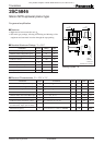
Marking Symbol: 7K
1.20±0.05
0.52±0.03
0 to 0.01
0.15 max.
5˚
0.15 min.
0.80
±0.050.15 min.
0.33
(0.40)(0.40)
12
3
5˚
0.80
±0.05
1.20±0.05
+0.05
–0.02
0.10
+0.05
–0.02
0.23
+0.05
–0.02
1: Base
2: Emitter
3: Collector
SSSMini3-F1 Package
Note) Measuring methods are based on JAPANESE INDUSTRIAL STANDARD JIS C 7030 measuring methods for transistors.
SSSMini3-F1 Package
This product complies with the RoHS Directive (EU 2002/95/EC).