


This product complies with the RoHS Directive (EU 2002/95/EC).
Transistors
1
Publication date: January 2003 SJC00189CED
Rank Q R S
h
FE1
85 to 170 120 to 240 170 to 340
2SD0592A (2SD592A)
Silicon NPN epitaxial planar type
For low-frequency output amplification
Complementary to 2SB0621A (2SB621A)
■ Features
• Large collector power dissipation P
C
• Low collector-emitter saturation voltage V
CE(sat)
■ Absolute Maximum Ratings T
a
= 25°C
Parameter Symbol Rating Unit
Collector-base voltage (Emitter open) V
CBO
60 V
Collector-emitter voltage (Base open) V
CEO
50 V
Emitter-base voltage (Collector open) V
EBO
5V
Collector current I
C
1 A
Peak collector current I
CP
1.5 A
Collector power dissipation P
C
750 mW
Junction temperature T
j
150 °C
Storage temperature T
stg
−55 to +150 °C
Parameter Symbol Conditions Min Typ Max Unit
Collector-base voltage (Emitter open) V
CBO
I
C
= 10 µA, I
E
= 060V
Collector-emitter voltage (Base open) V
CEO
I
C
= 2 mA, I
B
= 050V
Emitter-base voltage (Collector open) V
EBO
I
E
= 10 µA, I
C
= 05V
Collector-base cutoff current (Emitter open)
I
CBO
V
CB
= 20 V, I
E
= 0 0.1 µA
Forward current transfer ratio h
FE1
*
V
CE
= 10 V, I
C
= 500 mA 85 340
h
FE2
V
CE
= 5 V, I
C
= 1 A 50
Collector-emitter saturation voltage V
CE(sat)
I
C
= 500 mA, I
B
= 50 mA 0.2 0.4 V
Base-emitter saturation voltage V
BE(sat)
I
C
= 500 mA, I
B
= 50 mA 0.85 1.20 V
Transition frequency f
T
V
CB
= 10 V, I
E
= −50 mA, f = 200 MHz 200 MHz
Collector output capacitance C
ob
V
CB
= 10 V, I
E
= 0, f = 1 MHz 20 pF
(Common base, input open circuited)
■ Electrical Characteristics T
a
= 25°C ± 3°C
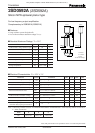
Unit: mm
1: Emitter
2: Collector
3: Base
TO-92-B1 Package
Note) 1. Measuring methods are based on JAPANESE INDUSTRIAL STANDARD JIS C 7030 measuring methods for transistors.
2.
*
: Rank classification
5.0
±0.2
0.7
±0.1
0.45
+0.15
–0.1
2.5
+0.6
–0.2
0.45
+0.15
–0.1
2.5
123
+0.6
–0.2
4.0
±0.2
5.1
±0.2
12.9
±0.5
2.3
±0.2
0.7
±0.2
Note) The part number in the parenthesis shows conventional part number.