


Switching Diodes
1
Publication date: November 2003 SKF00066BED
MA27111
Silicon epitaxial planar type
For high-speed switching circuits
■ Features
•
High-density mounting is possible
•
Short reverse recovery time t
rr
•
Small terminal capacitance C
t
■ Absolute Maximum Ratings T
a
= 25°C
Parameter Symbol Rating Unit
Reverse voltage V
R
80 V
Maximum peak reverse voltage V
RM
80 V
Forward current I
F
100 mA
Peak forward current I
FM
225 mA
Non-repetitive peak forward I
FSM
500 mA
surge current
*
Junction temperature T
j
150 °C
Storage temperature T
stg
−55 to +150 °C
■ Electrical Characteristics T
a
= 25°C ± 3°C
Parameter Symbol Conditions Min Typ Max Unit
Forward voltage V
F
I
F
= 100 mA 0.95 1.20 V
Reverse
voltage V
R
I
R
= 100 µA80
Reverse current I
R
V
R
= 75 V 100 nA
Terminal capacitance C
t
V
R
= 0 V, f = 1 MHz 0.6 2.0 pF
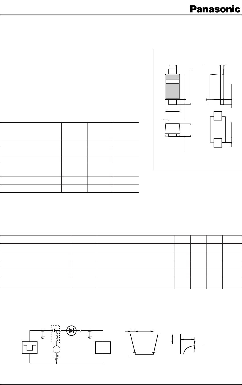
Reverse recovery time
*
t
rr
I
F
= 10 mA, V
R
= 6 V 3 ns
I
rr
= 0.1 I
R
, R
L
= 100 Ω
Bias Application Unit N-50BU
90%
Pulse Generator
(PG-10N)
R
s
= 50 Ω
Wave Form Analyzer
(SAS-8130)
R
i
= 50 Ω
t
p
= 2 µs
t
r
= 0.35 ns
δ = 0.05
I
F
= 10 mA
V
R
= 6 V
R
L
= 100 Ω
10%
Input Pulse Output Pulse
I
rr
= 0.1 I
R
t
r
t
p
t
rr
V
R
I
F
t
t
A
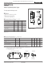
Unit: mm
Note) 1. Measuring methods are based on JAPANESE INDUSTRIAL STANDARD JIS C 7031 measuring methods for diodes.
2. Absolute frequency of input and output is 10 MHz.
3.
*
: t
rr
measurement circuit
1: Anode
2: Cathode
SSSMini2-F2 Package
Marking Symbol: S
5°
5°
0.27
2
1
1.40±0.05
0.52±0.03
1.00±0.05
0.60±0.05
0.15 min.
0 to 0.01
0.15 min.0.15 max.
+0.05
–0.02
0.13
+0.05
–0.02
Note)
*
: t = 1 s
This product complies with the RoHS Directive (EU 2002/95/EC).