


Schottky Barrier Diodes (SBD)
1
Publication date: November 2003 SKH00129AED
MA27E02
Silicon epitaxial planar type
For cellular phone
■ Features
• High-frequency wave detection is possible.
• Low forward voltage V
F
• Small terminal capacitance C
t
■ Absolute Maximum Ratings T
a
= 25°C
Parameter Symbol Rating Unit
Reverse voltage V
R
20 V
Maximum peak reverse voltage V
RM
20 V
Forward current I
F
35 mA
Peak forward current I
FM
100 mA
Junction temperature T
j
125 °C
Storage temperature T
stg
−55 to +125 °C
Parameter Symbol Conditions Min Typ Max Unit
Forward voltage V
F1
I
F
= 1 mA 0.40 V
V
F2
I
F
= 35 mA 1.0 V
Reverse current I
R
V
R
= 15 V 200 nA
Terminal capacitance C
t
V
R
= 0 V, f = 1 MHz 1.2 pF
Forward dynamic resistance r
f
I
F
= 5 mA 9 Ω
■ Electrical Characteristics T
a
=
25°C ±
3°C
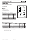
Marking Symbol: G
Unit: mm
5°
5°
0.27
2
1
1.40±0.05
0.52±0.03
1.00±0.05
0.60±0.05
0.15 min.
0 to 0.01
0.15 min.0.15 max.
+0.05
–0.02
0.13
+0.05
–0.02
Note) 1. Measuring methods are based on JAPANESE INDUSTRIAL STANDARD JIS C 7031 measuring methods for diodes.
2. This product is sensitive to electric shock (static electricity, etc.). Due attention must be paid on the charge of a human body
and the leakage of current from the operating equipment.
3. Rated input/output frequency: 2 GHz
1: Anode
2: Cathode
SSSMini2-F2 Package
This product complies with the RoHS Directive (EU 2002/95/EC).