


1
Publication date: March 2004 SKL00009BED
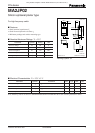
PIN diodes
Parameter Symbol Conditions Min Typ Max Unit
Forward voltage V
F
I
F
= 10 mA 1.0 V
Reverse current I
R
V
R
= 60 V 100 nA
Terminal capacitance C
t
V
R
= 1 V, f = 1 MHz 0.5 pF
Forward dynamic resistance r
f
I
F
= 10 mA, f = 100 MHz 2.0 Ω
■ Electrical Characteristics T
a
= 25°C ± 3°C
MA2JP02
Silicon epitaxial planar type
For high frequency switch
■ Features
• Small terminal capacitance C
t
• Small forward dynamic resistance r
f
• Miniature package and surface mounting type
■ Absolute Maximum Ratings T
a
= 25°C
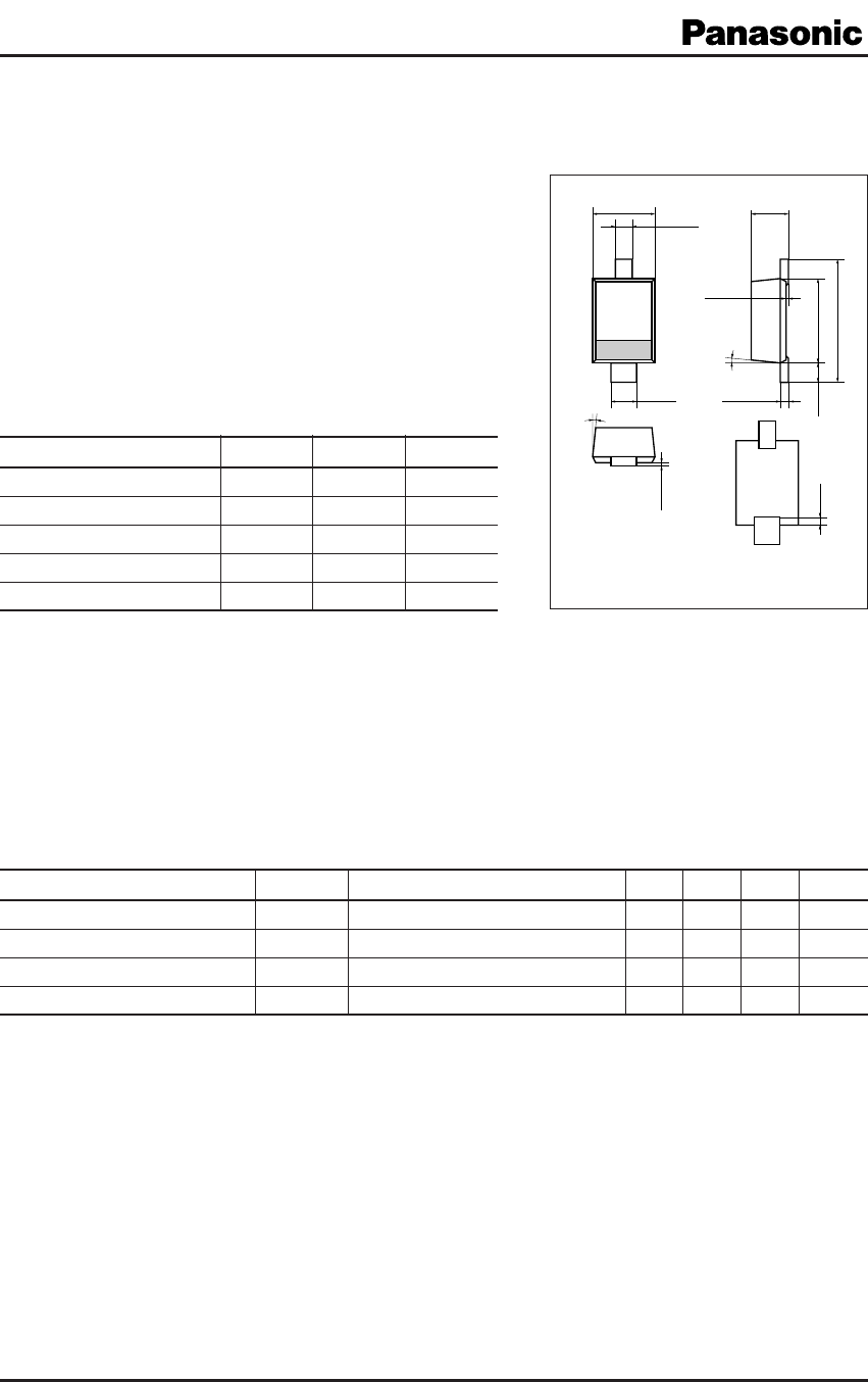
Unit: mm
Parameter Symbol Rating Unit
Reverse voltage V
R
60 V
Forward current I
F
100 mA
Power dissipation P
D
150 mW
Junction temperature T
j
150 °C
Storage temperature T
stg
−55 to +150 °C
1: Anode
2: Cathode
EIAJ: SC-76 SMini2-F1 Package
5˚
5˚
1.25
±0.1
0.7
±0.1
2.5
±0.2
1.7
±0.1
0.4
±0.1
0 to 0.1
(0.15)
0.16
0.5
±0.1
1
2
+0.1
–0.06
0.35
±0.1
0 to 0.1
Marking Symbol: 3F
Note) Measuring methods are based on JAPANESE INDUSTRIAL STANDARD JIS C 7031 measuring methods for diodes.
This product complies with the RoHS Directive (EU 2002/95/EC).