


Philips Semiconductors
User’s Manual - Preliminary -
P89LPC906/907/908
I/O PORTS
2003 Dec 8 36
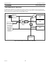
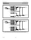
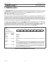
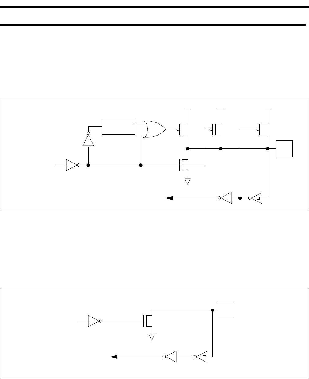
The third pullup is referred to as the "strong" pullup. This pullup is used to speed up low-to-high transitions on a quasi-bidirectional
port pin when the port latch changes from a logic 0 to a logic 1. When this occurs, the strong pullup turns on for two CPU clocks
quickly pulling the port pin high .
The quasi-bidirectional port configuration is shown in Figure 4-1.
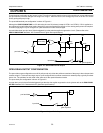
Although the P89LPC906/907/908 is a 3V device the pins are 5V-tolerant (except for XTAL1 and XTAL2). If 5V is applied to a
pin configured in quasi-bidirectional mode, there will be a current flowing from the pin to V
DD
causing extra power consumption.
Therefore, applying 5V to pins configured in quasi-bidirectional mode is discouraged.
A quasi-bidirectional port pin has a Schmitt-triggered input that also has a glitch suppression circuit. (Please refer to the
P89LPC906/907/908 datasheet, AC Characteristics for glitch filter specifications)
Figure 4-1: Quasi-Bidirectional Output
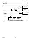
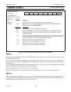
OPEN DRAIN OUTPUT CONFIGURATION
The open drain output configuration turns off all pullups and only drives the pulldown transistor of the port pin when the port latch
contains a logic 0. To be used as a logic output, a port configured in this manner must have an external pullup, typically a resistor
tied to V
DD
. The pulldown for this mode is the same as for the quasi-bidirectional mode.
The open drain port configuration is shown in Figure 4-2.
An open drain port pin has a Schmitt-triggered input that also has a glitch suppression circuit (please refer to the P89LPC906/
907/908 datasheet, AC Characteristics for glitch filter specifications).
Figure 4-2: Open Drain Output
weak
very
weak
strong
port
pin
V
DD
2 CPU
clock delay
input data
port latch data
V
DD
V
DD
glitch rejection
port
pin
input data
port latch data
glitch rejection