


Philips Semiconductors
User’s Manual - Preliminary -
P89LPC906/907/908
UART
2003 Dec 8 64
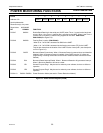
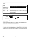
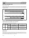
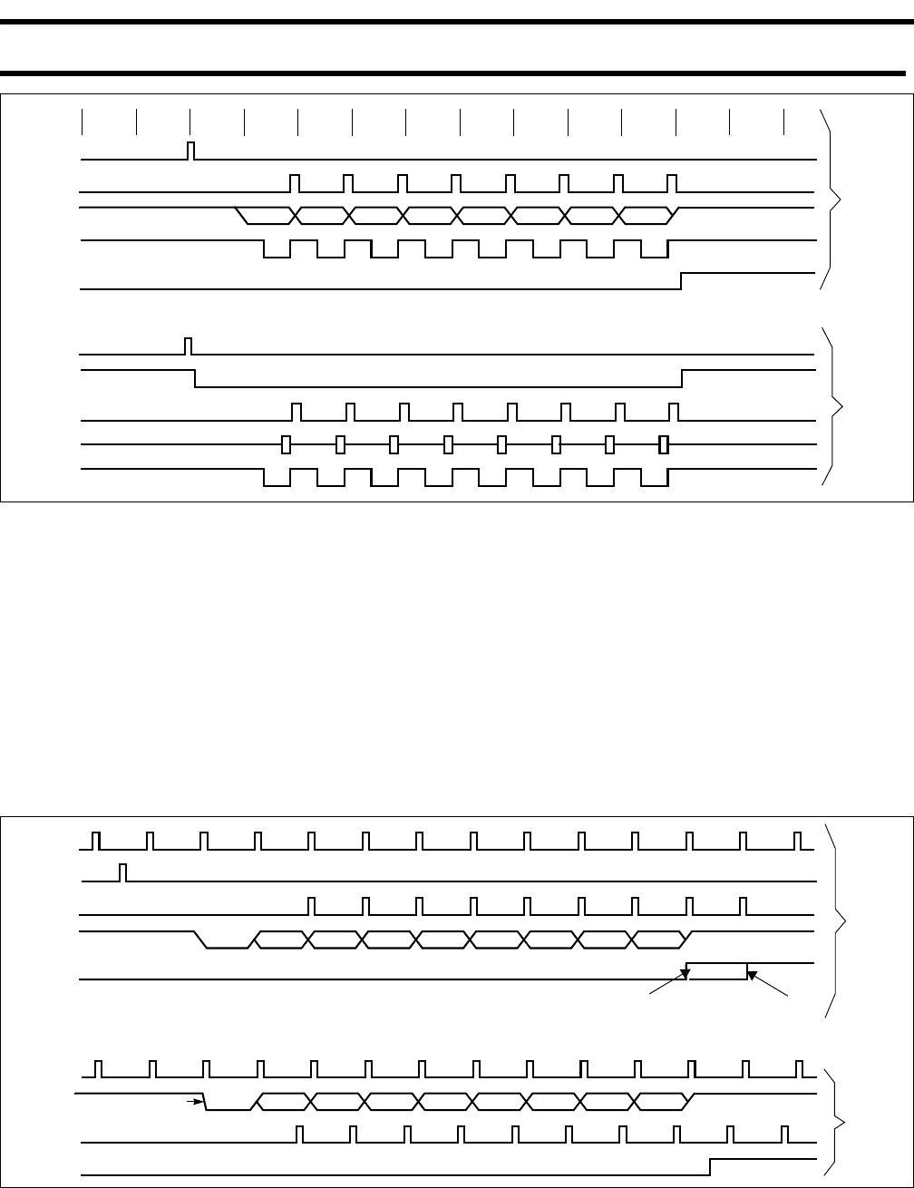
Figure 8-5: Serial Port Mode 0 (Double Buffering Must Be Disabled)
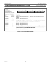
MORE ABOUT UART MODE 1
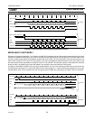
Reception is initiated by detecting a 1-to-0 transition on RxD. RxD is sampled at a rate 16 times the programmed baud rate. When
a transition is detected, the divide-by-16 counter is immediately reset. Each bit time is thus divided into 16 counter states. At the
7th, 8th, and 9th counter states, the bit detector samples the value of RxD. The value accepted is the value that was seen in at
least 2 of the 3 samples. This is done for noise rejection. If the value accepted during the first bit time is not 0, the receive circuits
are reset and the receiver goes back to looking for another 1-to-0 transition. This provides rejection of false start bits. If the start
bit proves valid, it is shifted into the input shift register, and reception of the rest of the frame will proceed.
The signal to load SBUF and RB8, and to set RI, will be generated if, and only if, the following conditions are met at the time the
final shift pulse is generated: RI = 0 and either SM2=0 or the received stop bit =1. If either of these two conditions is not met, the
received frame is lost. If both conditions are met, the stop bit goes into RB8, the 8 data bits go into SBUF, and RI is activated.
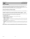
Figure 8-6: Serial Port Mode 1 (Only Single Transmit Buffering Case Is Shown)
Transmit
RxD (Data Out)
D0 D1 D5D2 D6D3 D4 D7
TxD (Shift Clock)
Shift
S1...S16 S1...S16 S1...S16 S1...S16S1...S16S1...S16 S1...S16 S1...S16 S1...S16 S1...S16S1...S16S1...S16 S1...S16
Write to SBUF
TI
Receive
D0 D1 D5D2 D6D3 D4 D7
TxD (Shift Clock)
Shift
Write to SCON (Clear RI)
RI
RxD
(Data In)
Transmit
Start Bit Stop Bit
TX Clock
Write to SBUF
Shift
TxD
TI
D0 D1 D5D2 D6D3 D4 D7
Receive
RX Clock
Shift
RI
Start Bit
Stop Bit
RxD
D0 D1 D5D2 D6D3 D4 D7
÷ 16 Reset
INTLO = 0
INTLO = 1