SH7211 Group
Data Transfer between On-chip RAM Areas with DMAC (Cycle-Stealing Mode)
REJ06B0732-0100/Rev.1.00 March 2008 Page 9 of 13
2.4 Register Settings for Sample Program
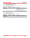
2.4.1 Clock Pulse Generator (CPG)
The settings of the clock pulse generator for the sample program are described in table 5.
Table 5 Settings of Clock Pulse Generator
Register Name Address Setting Value Description
Frequency control
register (FRQCR)
H’FFFE0010 H’1303 CKOEN = “B’1”: output clocks
STC[1:0] = “B’00”: frequency multiplication
ratio of PLL circuit × 1
IFC[2:0] = “B’000”: internal clock × 1
PFC[2:0] = “B’011”: peripheral clock × 1/4
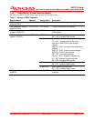
2.4.2 Standby Control Register
The settings of the standby control register for the sample program are described in table 6.
Table 6 Settings of Standby Control Register
Register Name Address Setting Value Description
Standby control
register 2 (STBCR2)
H’FFFE0018 H’00 MSTP8 = “B’0”: the DMAC operates


