


INSTRUCTION SET S3C8275X/F8275X/C8278X/F8278X/C8274X/F8274X
6-52
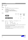
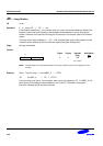
LDC/LDE — Load Memory
LDC/LDE dst,src
Operation: dst ← src
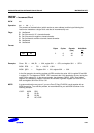
This instruction loads a byte from program or data memory into a working register or vice-versa.
The source values are unaffected. LDC refers to program memory and LDE to data memory. The
assembler makes 'Irr' or 'rr' values an even number for program memory and odd an odd number
for data memory.
Flags: No flags are affected.
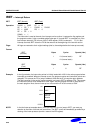
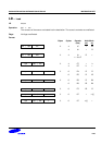
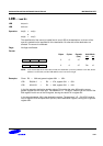
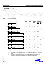
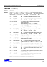
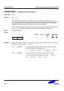
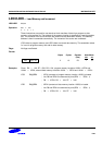
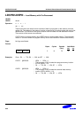
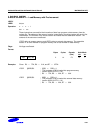
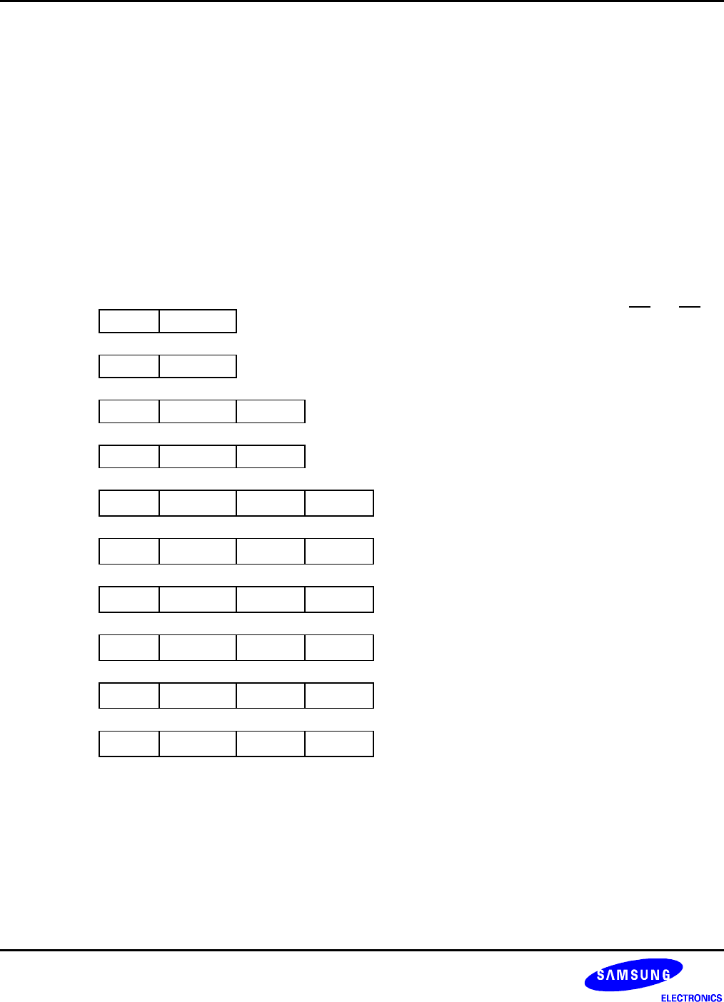
Format:
Bytes Cycles Opcode
(Hex)
Addr Mode
dst
src
1. opc
dst | src
2 10 C3 r Irr
2. opc
src | dst
2 10 D3 Irr r
3. opc
dst | src
XS
3 12 E7 r XS [rr]
4. opc
src | dst
XS
3 12 F7 XS [rr] r
5. opc
dst | src
XL
L
XL
H
4 14 A7 r XL [rr]
6. opc
src | dst
XL
L
XL
H
4 14 B7 XL [rr] r
7. opc dst | 0000
DA
L
DA
H
4 14 A7 r DA
8. opc
src | 0000
DA
L
DA
H
4 14 B7 DA r
9. opc
dst | 0001
DA
L
DA
H
4 14 A7 r DA
10. opc
src | 0001
DA
L
DA
H
4 14 B7 DA r
NOTES:
1. The source (src) or working register pair [rr] for formats 5 and 6 cannot use register pair 0–1.
2. For formats 3 and 4, the destination address 'XS [rr]' and the source address 'XS [rr]' are each
one byte.
3. For formats 5 and 6, the destination address 'XL [rr] and the source address 'XL [rr]' are each two
bytes.
4. The DA and r source values for formats 7 and 8 are used to address program memory; the
second set of values, used in formats 9 and 10, are used to address data memory.