


RESET and POWER-DOWN S3C8275X/F8275X/C8278X/F8278X/C8274X/F8274X
8-2
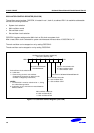
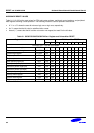
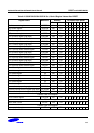
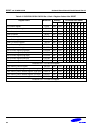
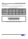
HARDWARE RESET VALUES
Table 8-1, 8-2, 8-3 list the reset values for CPU and system registers, peripheral control registers, and peripheral
data registers following a reset operation. The following notation is used to represent reset values:
• A "1" or a "0" shows the reset bit value as logic one or logic zero, respectively.
• An "x" means that the bit value is undefined after a reset.
• A dash ("–") means that the bit is either not used or not mapped, but read 0 is the bit value.
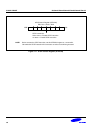
Table 8-1. S3C8275X/C8278X/C8274X Set 1 Register and Values After RESET
Register Name Mnemonic Address Bit Values After RESET
DecHex7654 3 2 10
Locations D0H – D2H are not mapped.
Basic timer control register BTCON 211 D3H 0000 0 0 00
System clock control register CLKCON 212 D4H 0
−
−
0 0
− −
−
System flags register FLAGS 213 D5H x x x x x x 0 0
Register pointer 0 RP0 214 D6H 1100 0
− −
−
Register pointer 1 RP1 215 D7H 1100 1
− −
−
Stack pointer (high byte) SPH 216 D8H x x x x x x x x
Stack pointer (low byte) SPL 217 D9H x x x x x x x x
Instruction pointer (high byte) IPH 218 DAH x x x x x x x x
Instruction pointer (low byte) IPL 219 DBH x x x x x x x x
Interrupt request register IRQ 220 DCH 0000 0 0 00
Interrupt mask register IMR 221 DDH x x x x x x x x
System mode register SYM 222 DEH 0
−
−
x x x 0 0
Register page pointer PP 223 DFH 0000 0 0 00