


S3C8275X/F8275X/C8278X/F8278X/C8274X/F8274X LCD CONTROLLER/DRIVER
13-3
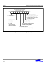
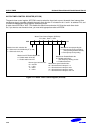
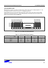
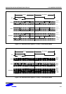
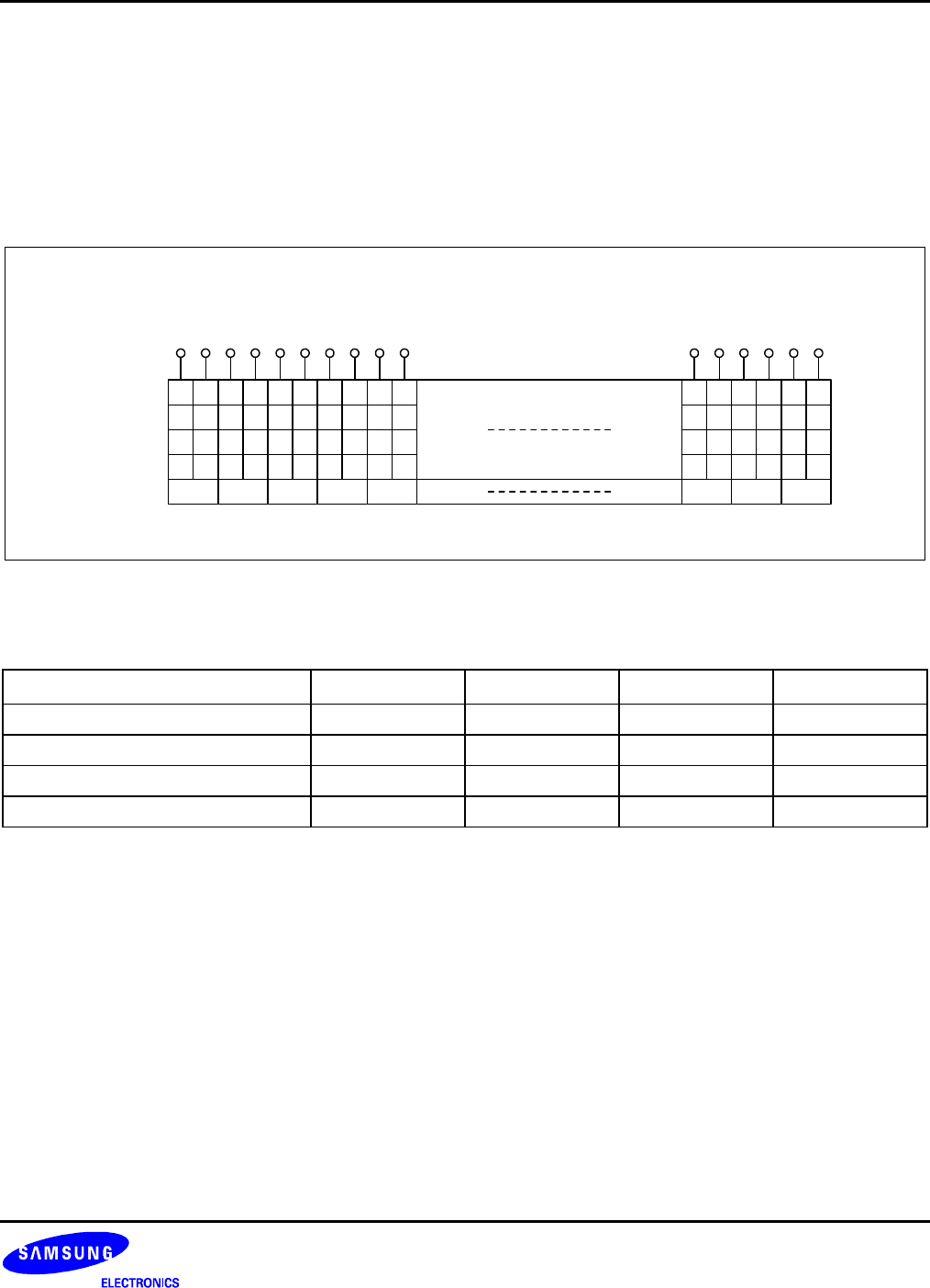
LCD RAM ADDRESS AREA
RAM addresses of page 2 are used as LCD data memory. When the bit value of a display segment is "1", the
LCD display is turned on; when the bit value is "0", the display is turned off.
Display RAM data are sent out through segment pins SEG0−SEG31 using a direct memory access (DMA)
method that is synchronized with the f
LCD
signal. RAM addresses in this location that are not used for LCD
display can be allocated to general-purpose use.
COM0
COM1
COM2
COM3
b0 b4 b0 b4 b0 b4 b0 b4 b0 b4
b1 b5
b2 b6
b3 b7
b1 b5
b2 b6
b3 b7
b1 b5
b2 b6
b3 b7
b1 b5
b2 b6
b3 b7
b1 b5
b2 b6
b3 b7
200H 201H 202H 203H 204H
b0 b4 b0 b4 b0 b4
b1 b5
b2 b6
b3 b7
b1 b5
b2 b6
b3 b7
b1 b5
b2 b6
b3 b7
20DH 20EH 20FH
SEG0
SEG1
SEG2
SEG3
SEG4
SEG5
SEG6
SEG7
SEG8
SEG9
SEG26
SEG27
SEG28
SEG29
SEG30
SEG31
Figure 13-3. LCD Display Data RAM Organization
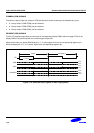
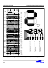
Table 13-1. LCD Clock Signal Frame Frequency
LCDCK Frequency (f
LCD
)
Static 1/2 Duty 1/3 Duty 1/4 Duty
64 Hz 64 32 21 16
128 Hz 128 64 43 32
256Hz 256 128 85 64
512 Hz 512 256 171 128