


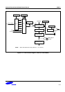
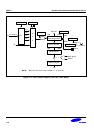
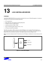
LCD CONTROLLER/DRIVER S3C8275X/F8275X/C8278X/F8278X/C8274X/F8274X
13-4
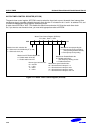
LCD CONTROL REGISTER (LCON)
A LCON is located in set 1, bank 1, at address E0H, and is read/write addressable using Register addressing
mode. It has the following control functions.
• LCD duty and bias selection
• LCD clock selection
• LCD display control
• Internal/External LCD dividing resistors selection
The LCON register is used to turn the LCD display on/off, to select duty and bias, to select LCD clock and control
the flow of the current to the dividing in the LCD circuit. Following a RESET, all LCON values are cleared to "0".
This turns off the LCD display, select 1/4 duty and 1/3 bias, select 64Hz for LCD clock, and Enable internal LCD
dividing resistors.
The LCD clock signal determines the frequency of COM signal scanning of each segment output. This is also
referred as the LCD frame frequency. Since the LCD clock is generated by watch timer clock (fw). The watch
timer should be enabled when the LCD display is turned on.
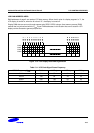
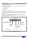
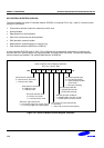
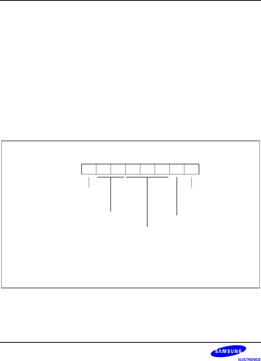
LCD Control Register (LCON)
E0H, Set 1, Bank 1, R/W
.7 .6 .5 .4 .3 .2 .1 .0MSB LSB
Internal LCD dividing register enable bit:
0 = Enable internal LCD dividing resistors
1 = Disable internal LCD dividing resistors
Not used for S3C8275X/C8278X/C8274X
LCD duty and bias selection bits:
000 = 1/4 duty, 1/3 bias
001 = 1/3 duty, 1/3 bias
010 = 1/3 duty, 1/2 bias
011 = 1/2 duty, 1/2 bias
1xx = Static
LCD display control bit:
0 = Turn display off
(Turn off the P-Tr)
1 = Turn display on
(Turn on the P-Tr)
LCD clock selection bits:
00 = fw/2
9
(64 Hz)
01 = fw/2
8
(128 Hz)
10 = fw/2
7
(256 Hz)
11 = fw/2
6
(512 Hz)
NOTES:
1. "x" means don't care.
2. When 1/2 bias is selected, the bias levels are set as V
LC0, VLC1(VLC2), and VSS.
Figure 13-4. LCD Control Register (LCON)