


S3F8275X/F8278X/F8274X FLASH MCU S3C8275X/F8275X/C8278X/F8278X/C8274X/F8274X
19-4
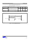
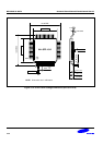
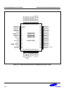
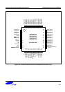
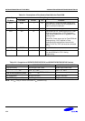
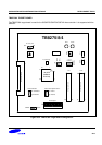
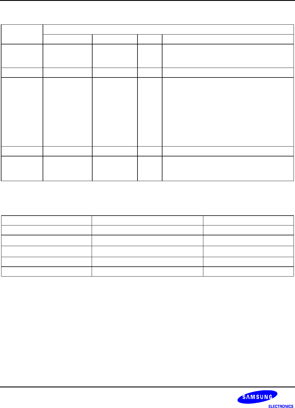
Table 19-1. Descriptions of Pins Used to Read/Write the Flash ROM
Main Chip During Programming
Pin Name Pin Name Pin No. I/O Function
VLC1 SDAT 7 I/O Serial data pin. Output port when reading and
input port when writing. Can be assigned as an
Input or push-pull output port.
VLC2 SCLK 8 I/O Serial clock pin. Input only pin.
TEST
V
PP
13 I S3F8278X/F8274X: Power supply pin for Flash
ROM cell reading/writing. 12.5V is applied in
Flash writing mode and 3.3V is applied in Flash
reading mode.
S3F8275X: Power supply pin for Flash ROM cell
reading/writing. 3.3V is applied in Flash
reading/writing mode because internal block
makes 12.5V. So, TEST pin must be connected
to V
DD
.
nRESET nRESET 16 I Chip initialization
V
DD
/V
SS
V
DD
/V
SS
9 / 10 I Power supply pin for logic circuit.
V
DD
should be tied to +3.3 V during
programming.
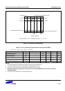
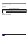
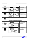
Table 19-2. Comparison of S3F8275X/F8278X/F8274X and S3C8275X/C8278X/C8274X Features
Characteristic S3F8275X/F8278X/F8274X S3C8275X/C8278X/C8274X
Program memory 16/8/4-Kbyte Flash ROM 16/8/4-Kbyte mask ROM
Operating voltage (V
DD
)
2.0 V to 3.6 V 2.0 V to 3.6 V
Flash ROM programming mode
V
DD
= 3.3 V, V
PP
(TEST)=12.5V
−
Pin configuration 64-QFP, 64-LQFP 64-QFP, 64-LQFP
Flash ROM programmability User Program multi time Programmed at the factory
NOTE: The V
PP
(Test) pin must be connected to V
DD
(S3F8275X only).