


REVISION DESCRIPTIONS
1. Electrical Data
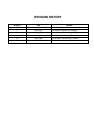
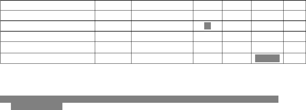
Table 17-12. A.C. Electrical Characteristics for Internal Flash ROM
(T
A
= − 25
°
C to + 85
°
C, V
DD
= 2.0 V to 3.6 V)
Parameter Symbol Conditions Min Typ Max Unit
Programming time
(1)
Ftp
−
30
− − µs
Chip erasing time
(2)
Ftp1
−
50
− −
ms
Sector erasing time
(3)
Ftp2
−
10
− −
ms
Data access time
Ft
RS
− −
25
−
ns
Number of writing/erasing FNwe
− − −
10,000
(4)
Times
NOTES:
1. The programming time is the time during which one byte (8-bit) is programmed.
2. The chip erasing time is the time during which all 16K byte block is erased.
3. The sector erasing time is the time during which all 128 byte block is erased.
4. Maximum number of writing/erasing is 10,000 times for full-flash(S3F8275) and 100 times for half-flash
(S3F8278X/F8274X).
5. The chip erasing is available in Tool Program Mode only.
2. Condition of Operating Voltage
Condition of operating voltage is modified “fx = 0 − 4.2MHz” to “fx = 0.4 − 4.2MHz” at 2.0V – 3.6V and
“fx = 0 − 8MHz” to “fx = 0.4 − 8MHz” at 2.5V − 3.6V in the page 17-2.
3. CHAPTHER 16. Embedded Flash Memory Interface
This chapter is modified for only S3F8275X.
4. CHAPTHER 7. Clock Circuit
The contents of OSCCON.7 should be changed “ 0 = Select normal circuit for sub oscillator” into “ 0 = Initial state”
in the page 4-21 and Figure 7-10.
It is added “NOTE: The OSCCON.7 should be maintained to “1”, during the sub oscillator operation.” In the page
4-21 and Figure 7-10.
The figure 7-7 is modified partly.