


S3C8275X/F8275X/C8278X/F8278X/C8274X/F8274X CONTROL REGISTER
4-1
4 CONTROL REGISTERS
OVERVIEW
In this chapter, detailed descriptions of the S3C8275X/C8278X/C8274X control registers are presented in an
easy-to-read format. You can use this chapter as a quick-reference source when writing application programs.
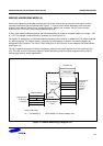
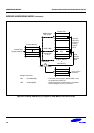
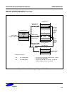
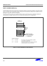
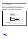
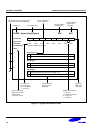
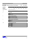
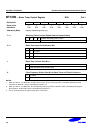
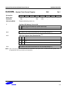
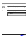
Figure 4-1 illustrates the important features of the standard register description format.
Control register descriptions are arranged in alphabetical order according to register mnemonic. More detailed
information about control registers is presented in the context of the specific peripheral hardware descriptions in
Part II of this manual.
Data and counter registers are not described in detail in this reference chapter. More information about all of the
registers used by a specific peripheral is presented in the corresponding peripheral descriptions in Part II of this
manual.
The locations and read/write characteristics of all mapped registers in the S3C8275X/C8278X/C8274X register
file are listed in Table 4-1. The hardware reset value for each mapped register is described in Chapter 8, "RESET
and Power-Down."
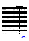
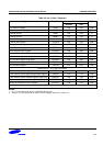
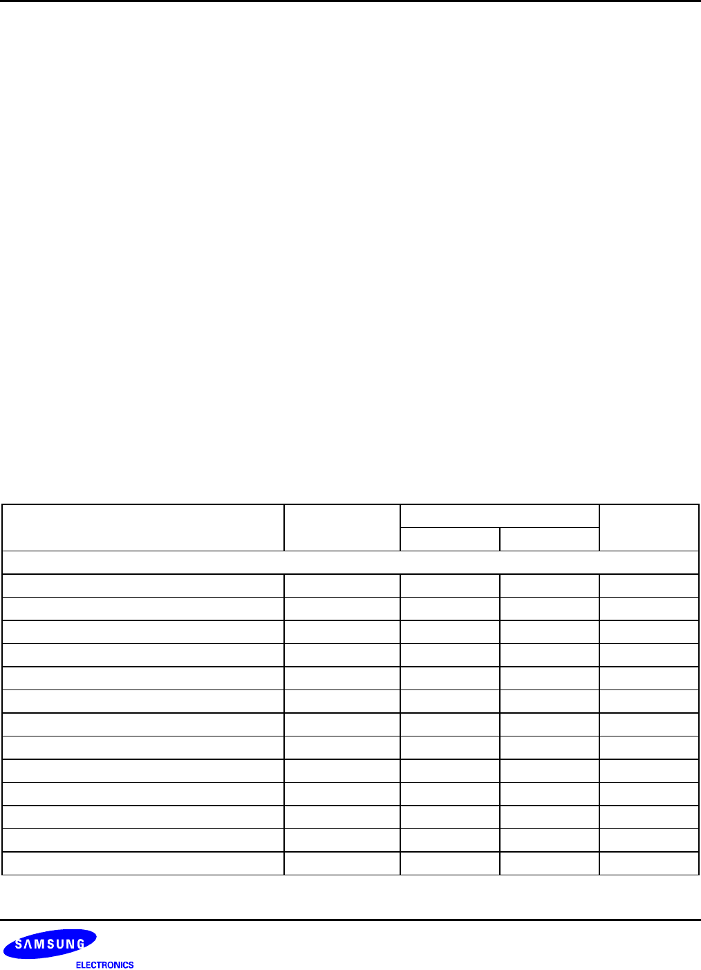
Table 4-1. Set 1 Registers
Register Name Mnemonic Address R/W
Decimal Hex
Locations D0H – D2H are not mapped.
Basic timer control register BTCON 211 D3H R/W
System clock control register CLKCON 212 D4H R/W
System flags register FLAGS 213 D5H R/W
Register pointer 0 RP0 214 D6H R/W
Register pointer 1 RP1 215 D7H R/W
Stack pointer (high byte) SPH 216 D8H R/W
Stack pointer (low byte) SPL 217 D9H R/W
Instruction pointer (high byte) IPH 218 DAH R/W
Instruction pointer (low byte) IPL 219 DBH R/W
Interrupt request register IRQ 220 DCH R
Interrupt mask register IMR 221 DDH R/W
System mode register SYM 222 DEH R/W
Register page pointer PP 223 DFH R/W