


S3C8275X/F8275X/C8278X/F8278X/C8274X/F8274X CONTROL REGISTER
4-13
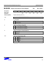
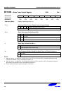
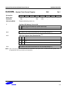
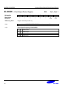
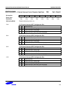
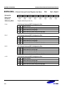
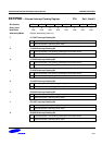
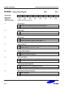
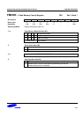
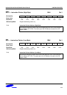
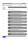
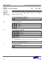
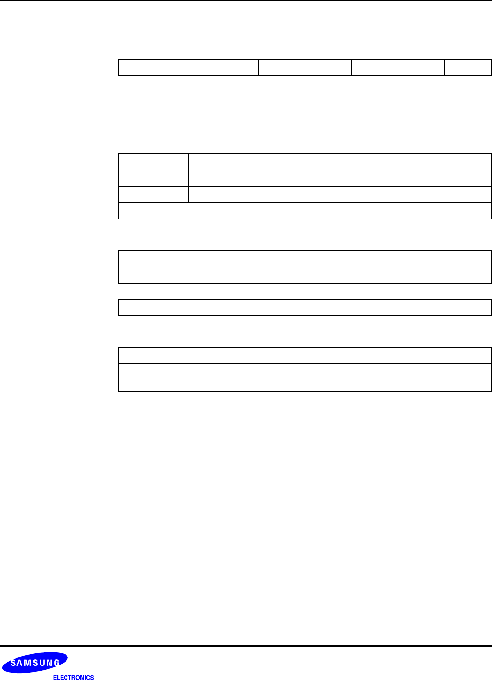
FMCON — Flash Memory Control Register F0H Set 1, Bank 1
Bit Identifier .7 .6 .5 .4 .3 .2 .1 .0
Reset Value
0 0 0 0 0 – – 0
Read/Write
R/W R/W R/W R/W R – – R/W
Addressing Mode
Register addressing mode only
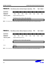
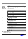
.7–.4 Flash Memory Mode Selection Bits
0 1 0 1 Programming mode
1 0 1 0 Sector erase mode
0 1 1 0 Hard lock mode
Other values Not available
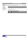
.3 Sector Erase Status Bit
0 Success sector erase
1 Fail sector erase
.2–.1
Not used for the S3F8275X/F8278X/F8274X
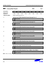
.0 Flash Operation Start Bit
0 Operation stop
1 Operation start (This bit will be cleared automatically just after the
corresponding operator completed).