


S3C8275X/F8275X/C8278X/F8278X/C8274X/F8274X CONTROL REGISTER
4-21
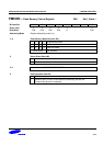
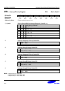
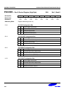
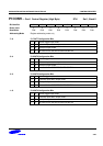
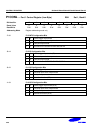
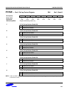
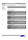
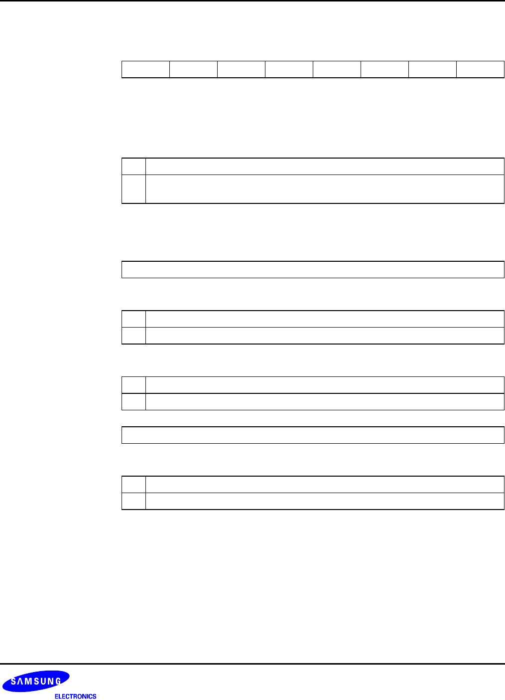
OSCCON — Oscillator Control Register E0H Set 1, Bank 0
Bit Identifier .7 .6 .5 .4 .3 .2 .1 .0
Reset Value
0 – – – 0 0 – 0
Read/Write
R/W – – – R/W R/W – R/W
Addressing Mode
Register addressing mode only
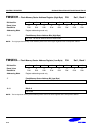
.7 Sub Oscillator Circuit Selection Bit
0 Initial state
1 Power saving circuit for sub oscillator (Automatically cleared to "0" when the
sub oscillator is stopped by OSCCON.2).
NOTES:
1. The OSCCON.7 must be maintained to “1”, during the sub oscillator operation.
2. A capacitor (0.1uF) should be connected between V
REG
and GND.
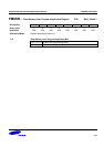
.6–.4
Not used for the S3C8275X/C8278X/C8274X
.3 Main Oscillator Control Bit
0 Main oscillator RUN
1 Main oscillator STOP
.2 Sub Oscillator Control Bit
0 Sub oscillator RUN
1 Sub oscillator STOP
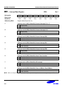
.1
Not used for the S3C8275X/C8278X/C8274X
.0 System Clock Selection Bit
0 Select main oscillator for system clock
1 Select sub oscillator for system clock