


- 14 -
datasheet DDR3L SDRAM
Rev. 1.0
Unbuffered DIMM
11.2 V
REF
Tolerances
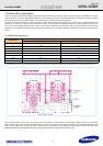
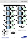
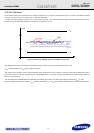
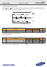
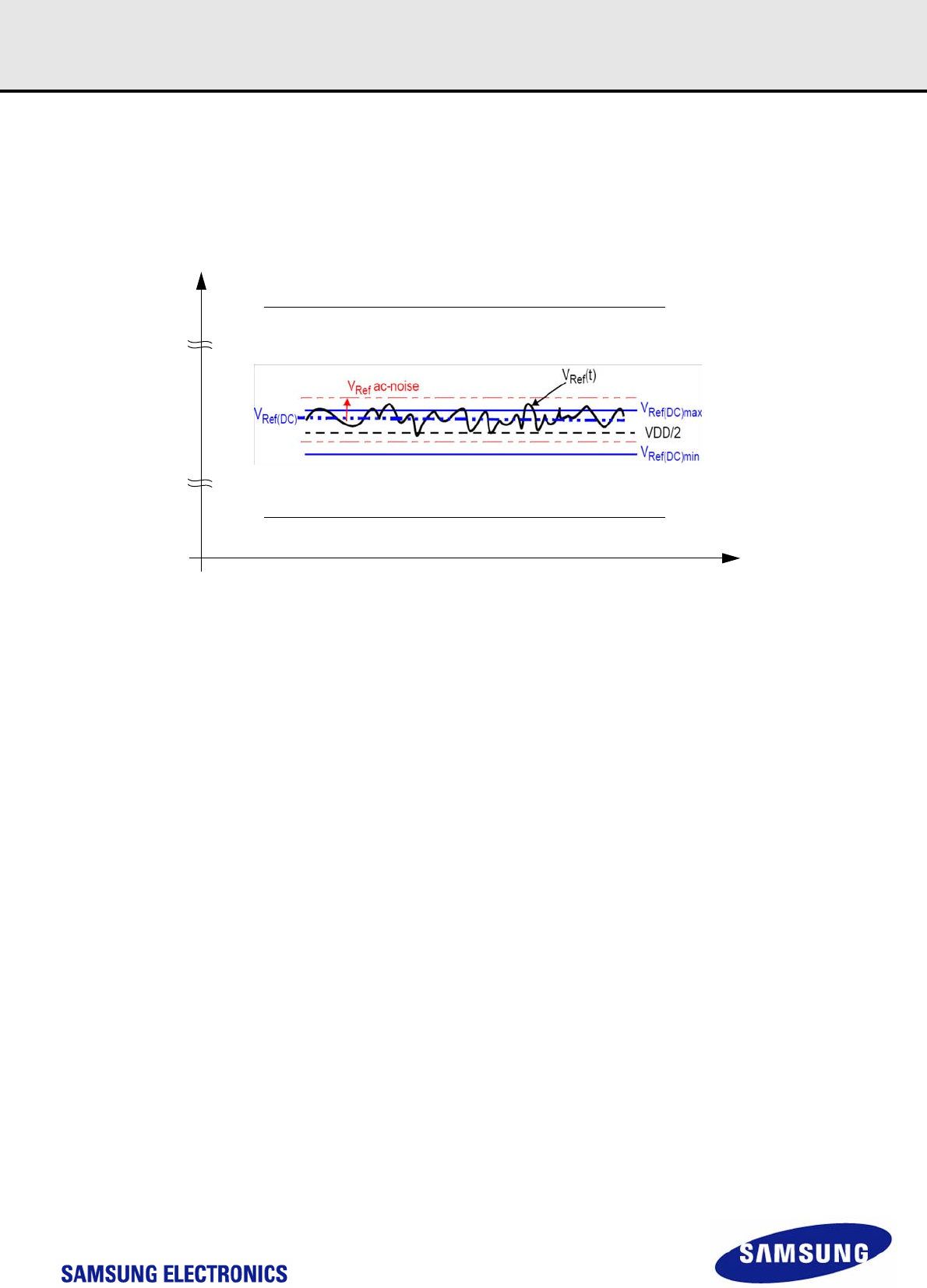
The dc-tolerance limits and ac-noise limits for the reference voltages V
REFCA
and V
REFDQ
are illustrate in Figure 2. It shows a valid reference voltage
V
REF
(t) as a function of time. (V
REF
stands for V
REFCA
and V
REFDQ
likewise).
V
REF
(DC) is the linear average of V
REF
(t) over a very long period of time (e.g. 1 sec). This average has to meet the min/max requirements of V
REF
. Fur-
thermore V
REF
(t) may temporarily deviate from V
REF
(DC) by no more than ± 1% V
DD
.
Figure 2. Illustration of VREF(DC) tolerance and VREF ac-noise limits
The voltage levels for setup and hold time measurements V
IH
(AC), V
IH
(DC), V
IL
(AC) and V
IL
(DC) are dependent on V
REF
.
"V
REF
" shall be understood as V
REF
(DC), as defined in Figure 2.
This clarifies, that dc-variations of V
REF
affect the absolute voltage a signal has to reach to achieve a valid high or low level and therefore the time to
which setup and hold is measured. System timing and voltage budgets need to account for V
REF
(DC) deviations from the optimum position within the
data-eye of the input signals.
This also clarifies that the DRAM setup/hold specification and derating values need to include time and voltage associated with V
REF
ac-noise.
Timing and voltage effects due to ac-noise on V
REF
up to the specified limit (+/-1% of V
DD
) are included in DRAM timings and their associated deratings.
voltage
V
DD
V
SS
time