


- 26 -
datasheet DDR3L SDRAM
Rev. 1.0
Unbuffered DIMM
16. Electrical Characteristics and AC timing
[0 °C<T
CASE
≤95 °C, V
DDQ
= 1.35V(1.28V~1.45V) & 1.5V(1.425V~1.575V); V
DD
= 1.35V(1.28V~1.45V) & 1.5V(1.425V~1.575V)]
16.1 Refresh Parameters by Device Density
NOTE :
1. Users should refer to the DRAM supplier data sheet and/or the DIMM SPD to determine if DDR3 SDRAM devices support the following options or requirements referred to in
this material.
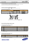
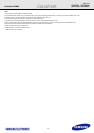
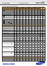
16.2 Speed Bins and CL, tRCD, tRP, tRC and tRAS for Corresponding Bin
16.3 Speed Bins and CL, tRCD, tRP, tRC and tRAS for corresponding Bin
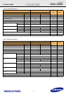
DDR3 SDRAM Speed Bins include tCK, tRCD, tRP, tRAS and tRC for each corresponding bin.
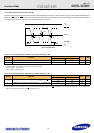
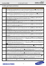
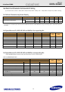
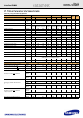
[ Table 17 ] DDR3-800 Speed Bins
Parameter Symbol 1Gb 2Gb 4Gb 8Gb Units NOTE
All Bank Refresh to active/refresh cmd time tRFC 110 160 300 350 ns
Average periodic refresh interval tREFI
0 °C ≤ T
CASE
≤ 85°C
7.8 7.8 7.8 7.8 µs
85 °C < T
CASE
≤ 95°C
3.9 3.9 3.9 3.9 µs 1
Speed DDR3-800 DDR3-1066 DDR3-1333 DDR3-1600
Units NOTEBin (CL - tRCD - tRP) 6-6-6 7-7-7 9-9-9 11-11-11
Parameter min min min min
CL 6 7911tCK
tRCD 15 13.13 13.5 13.75 ns
tRP 15 13.13 13.5 13.75 ns
tRAS 37.5 37.5 36 35 ns
tRC 52.5 50.63 49.5 48.75 ns
tRRD 10 7.5 6.0 6.0 ns
tFAW 40 37.5 30 30 ns
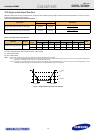
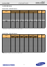
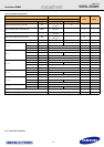
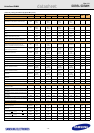
Speed DDR3-800
Units NOTECL-nRCD-nRP 6 - 6 - 6
Parameter Symbol min max
Internal read command to first data tAA 15 20 ns
ACT to internal read or write delay time tRCD 15 - ns
PRE command period tRP 15 - ns
ACT to ACT or REF command period tRC 52.5 - ns
ACT to PRE command period tRAS 37.5 9*tREFI ns
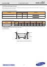
CL = 6 / CWL = 5 tCK(AVG) 2.5 3.3 ns 1,2,3
Supported CL Settings 6 nCK
Supported CWL Settings 5 nCK