


- 6 -
datasheet DDR3L SDRAM
Rev. 1.0
Unbuffered DIMM
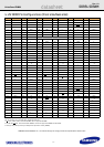
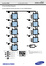
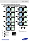
5. Pin Description
NOTE :
* The V
DD
and V
DDQ
pins are tied common to a single power-plane on these designs.
** DM8, DQS8 and DQS
8 are for ECC UDIMM only.
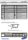
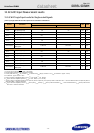
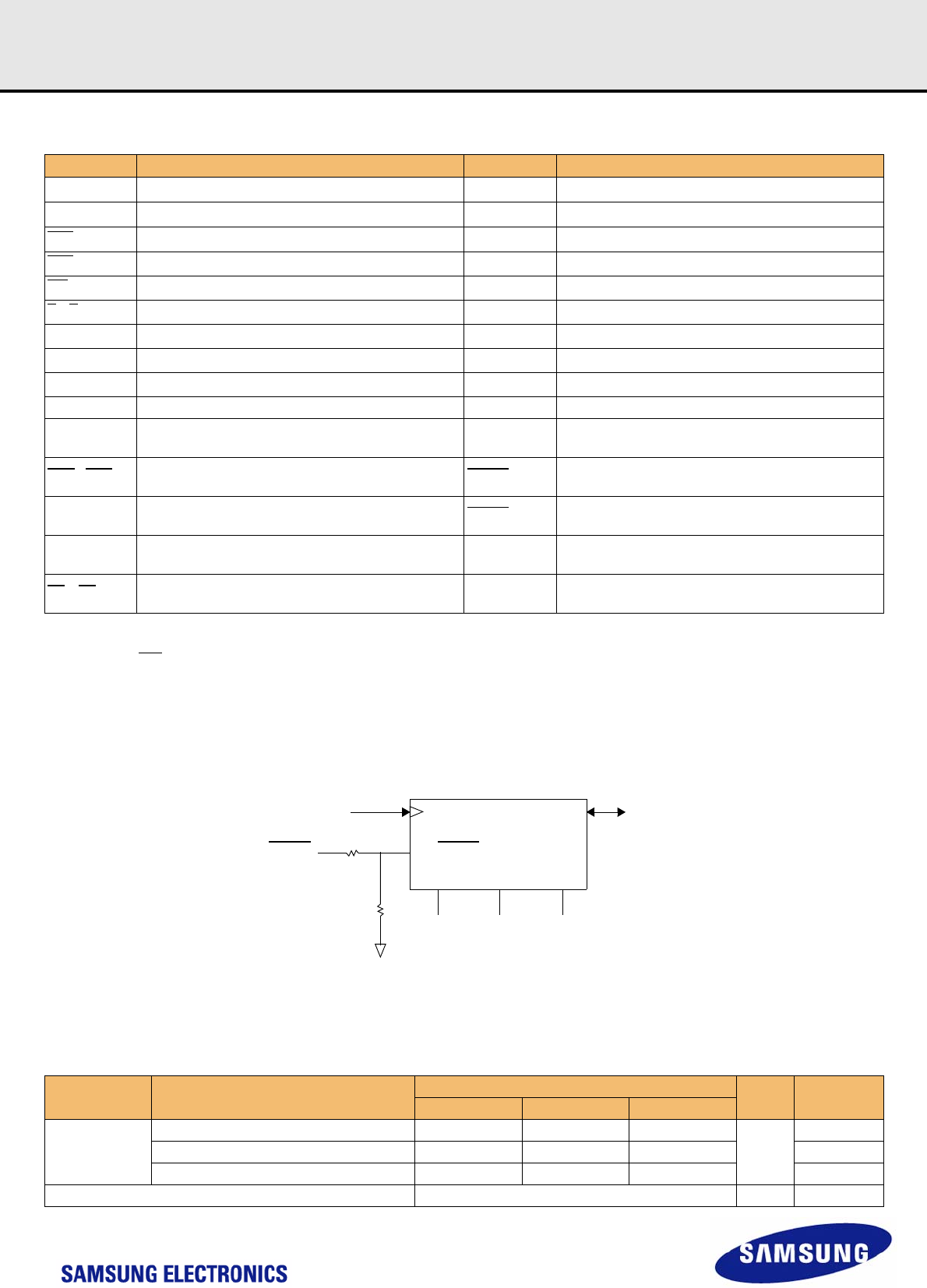
6. SPD and Thermal Sensor for ECC UDIMMs
On DIMM thermal sensor will provide DRAM temperature readout through a integrated thermal sensor.
NOTE :
1. Raw Cards D (1Rx8 ECC) and E (2Rx8 ECC) support a thermal sensor.
2. When the SPD and the thermal sensor are placed on the module, R1 is placed but R2 is not.
When only the SPD is placed on the module, R2 is placed but R1 is not.
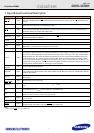
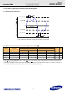
[ Table 1 ] Temperature Sensor Characteristics
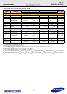
Pin Name Description Pin Name Description
A0-A14 SDRAM address bus SCL
I
2
C serial bus clock for EEPROM
BA0-BA2 SDRAM bank select SDA
I
2
C serial bus data line for EEPROM
RAS
SDRAM row address strobe SA0-SA2
I
2
C serial address select for EEPROM
CAS
SDRAM column address strobe
V
DD
*
SDRAM core power supply
WE
SDRAM write enable
V
DDQ
*
SDRAM I/O Driver power supply
S
0, S1 DIMM Rank Select Lines
V
REFDQ
SDRAM I/O reference supply
CKE0,CKE1 SDRAM clock enable lines
V
REFCA
SDRAM command/address reference supply
ODT0, ODT1 On-die termination control lines
V
SS
Power supply return (ground)
DQ0 - DQ63 DIMM memory data bus
V
DDSPD
Serial EEPROM positive power supply
CB0 - CB7 DIMM ECC check bits NC Spare Pins(no connect)
DQS0 - DQS8
SDRAM data strobes
(positive line of differential pair)
TEST
Used by memory bus analysis tools
(unused on memory DIMMs)
DQS
0-DQS8
SDRAM differential data strobes
(negative line of differential pair)
RESET Set DRAMs Known State
DM0-DM8
SDRAM data masks/high data strobes
(x8-based x72 DIMMs)
EVENT
Reserved for optional temperature-sensing hardware
CK0, CK1
SDRAM clocks
(positive line of differential pair)
V
TT
SDRAM I/O termination supply
CK
0, CK1
SDRAM clocks
(negative line of differential pair)
RFU Reserved for future use
Grade Range
Temperature Sensor Accuracy
Units NOTE
Min. Typ. Max.
B
75 < Ta < 95 - +/- 0.5 +/- 1.0
°C
-
40 < Ta < 125 - +/- 1.0 +/- 2.0 -
-20 < Ta < 125 - +/- 2.0 +/- 3.0 -
Resolution 0.25 °C /LSB -
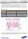
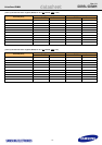
SCL
SDA
WP/EVENT
SA0 SA1 SA2
SA0 SA1 SA2
EVENT
R1
0 Ω
R2
0 Ω