


- 8 -
datasheet DDR3L SDRAM
Rev. 1.0
Unbuffered DIMM
7.1 Address Mirroring Feature
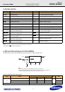
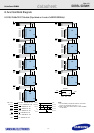
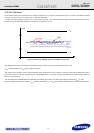
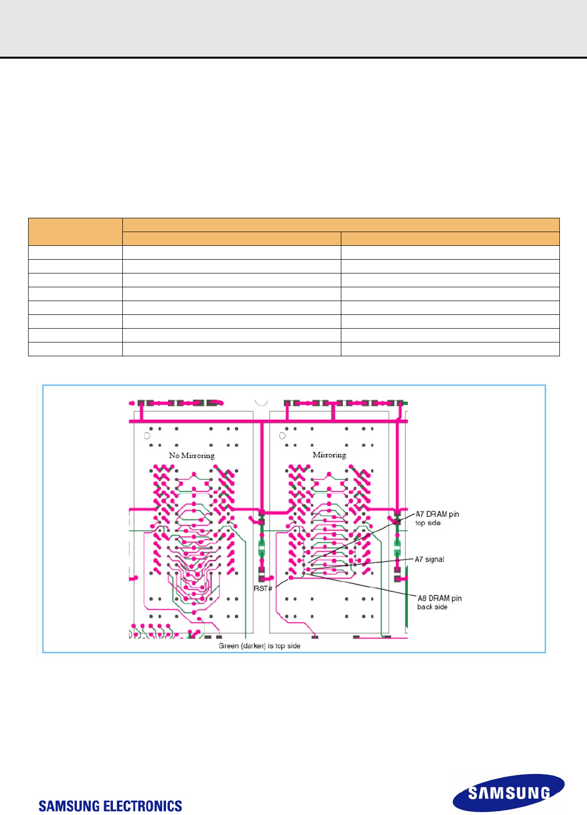
Figure 1. Wiring Differences for Mirrored and Non-Mirrored Addresses
There is a via grid located under the DRAMs for wiring the CA sign
als (address, bank address, command, and control lines) to the DRAM pins. The length
of the traces from the vias to the DRAMs places limitations on the bandwidth of the module. The shorter these traces, the higher the bandwidth. To extend
the bandwidth of the CA bus for DDR3 modules, a scheme was defined to reduce the length of these traces.
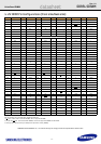
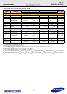
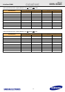
The pins on the DRAM are defined in a manner that allows for these short trace lengths. The CA bus pins in Columns 2 and 8, ignoring the mechanical
support pins, do not have any special functions (secondary functions). This allows the most flexibility with these pins. These are address pins A3, A4, A5,
A6, A7, A8 and bank address pins BA0 and BA1. Refer to Table . Rank 0 DRAM pins are wired straight, with no mismatch between the connector pin
assignment and the DRAM pin assignment. Some of the Rank 1 DRAM pins are cross wired as defined in the table. Pins not listed in the table are wired
straight.
7.1.1 DRAM Pin Wiring Mirroring
Figure 1illustrates the wiring in both the mirrored and non-mirrored case. The lengths of the traces to the DRAM pins, is obviously shorter. The via grid is smaller as well.
Since the cross-wired pins have no secondary functions, there is no problem in normal operation. Any data written is read the same way. There are limi-
tations however. When writing to the internal registers with a "load mode" operation, the specific address is required. See the DDR3 UDIMM SPD specifi-
cation for these details. The controller must read the SPD and have the capability of de-mirroring the address when accessing the second rank.
SAMSUNG DDR3 dual rank UDIMM R/C B(2Rx8) and R/C E(2Rx8) Modules are using Mirrored Addresses mode.
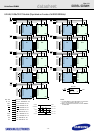
Connector Pin
DRAM Pin
Rank 0 Rank 1
A3 A3 A4
A4 A4 A3
A5 A5 A6
A6 A6 A5
A7 A7 A8
A8 A8 A7
BA0 BA0 BA1
BA1 BA1 BA0