


- 17 -
Unbuffered SODIMM datasheet DDR3 SDRAM
Rev. 1.0
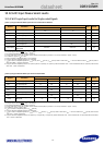
12. DIMM IDD specification definition
Symbol Description
IDD0
Operating One Bank Active-Precharge Current
CKE: High; External clock: On; tCK, nRC, nRAS, CL: Refer to Component Datasheet for detail pattern ; BL: 8
1)
; AL: 0; CS: High between ACT and PRE;
Command, Address, Bank Address Inputs: partially toggling ; Data IO: FLOATING; DM:stable at 0; Bank Activity: Cycling with one bank active at a time:
0,0,1,1,2,2,... ; Output Buffer and RTT: Enabled in Mode Registers
2)
; ODT Signal: stable at 0; Pattern Details: Refer to Component Datasheet for detail pat-
tern
IDD1
Operating One Bank Active-Read-Precharge Current
CKE: High; External clock: On; tCK, nRC, nRAS, nRCD, CL: Refer to Component Datasheet for detail pattern ; BL: 8
1)
; AL: 0; CS: High between ACT, RD
and PRE; Command, Address, Bank Address Inputs, Data IO: partially toggling ; DM:stable at 0; Bank Activity: Cycling with one bank active at a time:
0,0,1,1,2,2,... ; Output Buffer and RTT: Enabled in Mode Registers
2)
; ODT Signal: stable at 0; Pattern Details: Refer to Component Datasheet for detail pat-
tern
IDD2N
Precharge Standby Current
CKE: High; External clock: On; tCK, CL: Refer to Component Datasheet for detail pattern ; BL: 8
1)
; AL: 0; CS: stable at 1; Command, Address, Bank
Address Inputs: partially toggling ; Data IO: FLOATING; DM:stable at 0; Bank Activity: all banks closed; Output Buffer and RTT: Enabled in Mode
Registers
2)
; ODT Signal: stable at 0; Pattern Details: Refer to Component Datasheet for detail pattern
IDD2P0
Precharge Power-Down Current Slow Exit
CKE: Low; External clock: On; tCK, CL: Refer to Component Datasheet for detail pattern ; BL: 8
1)
; AL: 0; CS: stable at 1; Command, Address, Bank
Address Inputs: stable at 0; Data IO: FLOATING; DM:stable at 0; Bank Activity: all banks closed; Output Buffer and RTT: Enabled in Mode Registers
2)
;
ODT Signal: stable at 0; Precharge Power Down Mode: Slow Exit
3)
IDD2P1
Precharge Power-Down Current Fast Exit
CKE: Low; External clock: On; tCK, CL: Refer to Component Datasheet for detail pattern ; BL: 8
1)
; AL: 0; CS: stable at 1; Command, Address, Bank
Address Inputs: stable at 0; Data IO: FLOATING; DM:stable at 0; Bank Activity: all banks closed; Output Buffer and RTT: Enabled in Mode Registers
2)
;
ODT Signal: stable at 0; Precharge Power Down Mode: Fast Exit
3)
IDD2Q
Precharge Quiet Standby Current
CKE: High; External clock: On; tCK, CL: Refer to Component Datasheet for detail pattern ; BL: 8
1)
; AL: 0; CS: stable at 1; Command, Address, Bank
Address Inputs: stable at 0; Data IO: FLOATING; DM:stable at 0;Bank Activity: all banks closed; Output Buffer and RTT: Enabled in Mode Registers
2)
;
ODT Signal: stable at 0
IDD3N
Active Standby Current
CKE: High; External clock: On; tCK, CL: Refer to Component Datasheet for detail pattern ; BL: 8
1)
; AL: 0; CS: stable at 1; Command, Address, Bank
Address Inputs: partially toggling ; Data IO: FLOATING; DM:stable at 0;Bank Activity: all banks open; Output Buffer and RTT: Enabled in Mode
Registers
2)
; ODT Signal: stable at 0; Pattern Details: Refer to Component Datasheet for detail pattern
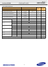
IDD3P
Active Power-Down Current
CKE: Low; External clock: On; tCK, CL: Refer to Component Datasheet for detail pattern ; BL: 8
1)
; AL: 0; CS: stable at 1; Command, Address, Bank
Address Inputs: stable at 0; Data IO: FLOATING;DM:stable at 0; Bank Activity: all banks open; Output Buffer and RTT: Enabled in Mode Registers
2)
; ODT
Signal: stable at 0
IDD4R
Operating Burst Read Current
CKE: High; External clock: On; tCK, CL: Refer to Component Datasheet for detail pattern ; BL: 8
1)
; AL: 0; CS: High between RD; Command, Address,
Bank Address Inputs: partially toggling ; Data IO: seamless read data burst with different data between one burst and the next one ; DM:stable at 0; Bank
Activity: all banks open, RD commands cycling through banks: 0,0,1,1,2,2,... ; Output Buffer and RTT: Enabled in Mode Registers
2)
; ODT Signal: stable
at 0; Pattern Details: Refer to Component Datasheet for detail pattern
IDD4W
Operating Burst Write Current
CKE: High; External clock: On; tCK, CL: Refer to Component Datasheet for detail pattern ; BL: 8
1)
; AL: 0; CS: High between WR; Command, Address,
Bank Address Inputs: partially toggling ; Data IO: seamless write data burst with different data between one burst and the next one ; DM: stable at 0; Bank
Activity: all banks open, WR commands cycling through banks: 0,0,1,1,2,2,... ; Output Buffer and RTT: Enabled in Mode Registers
2)
; ODT Signal: stable
at HIGH
; Pattern Details: Refer to Component Datasheet for detail pattern
IDD5B
Burst Refresh Current
CKE: High; External clock: On; tCK, CL, nRFC: Refer to Component Datasheet for detail pattern ; BL: 8
1)
; AL: 0; CS: High between REF; Command,
Address, Bank Address Inputs: partially toggling ; Data IO: FLOATING;DM:stable at 0; Bank Activity: REF command every nRFC ; Output Buffer and
RTT: Enabled in Mode Registers
2)
; ODT Signal: stable at 0; Pattern Details: Refer to Component Datasheet for detail pattern
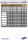
IDD6
Self Refresh Current: Normal Temperature Range
TCASE: 0 - 85°C; Auto Self-Refresh (ASR): Disabled
4)
; Self-Refresh Temperature Range (SRT): Normal
5)
; CKE: Low; External clock: Off; CK and CK:
LOW; CL: Refer to Component Datasheet for detail pattern ; BL: 8
1)
; AL: 0; CS, Command, Address, Bank Address, Data IO: FLOATING;DM:stable at 0;
Bank Activity: Self-Refresh operation; Output Buffer and RTT: Enabled in Mode Registers
2)
; ODT Signal: FLOATING
IDD6ET
Self-Refresh Current: Extended Temperature Range (optional)
6)
TCASE: 0 - 95°C; Auto Self-Refresh (ASR): Disabled
4)
; Self-Refresh Temperature Range (SRT): Extended
5)
; CKE: Low; External clock: Off; CK and CK:
LOW; CL: Refer to Component Datasheet for detail pattern ; BL: 8
1)
; AL: 0; CS, Command, Address, Bank Address, Data IO: FLOATING;DM:stable at 0;
Bank Activity: Extended Temperature Self-Refresh operation; Output Buffer and RTT: Enabled in Mode Registers
2)
; ODT Signal: FLOATING
IDD7
Operating Bank Interleave Read Current
CKE: High; External clock: On; tCK, nRC, nRAS, nRCD, nRRD, nFAW, CL: Refer to Component Datasheet for detail pattern ; BL: 8
1)
; AL: CL-1; CS: High
between ACT and RDA; Command, Address, Bank Address Inputs: partially toggling ; Data IO: read data bursts with different data between one burst and
the next one ; DM:stable at 0; Bank Activity: two times interleaved cycling through banks (0, 1, ...7) with different addressing ; Output Buffer and RTT:
Enabled in Mode Registers
2)
; ODT Signal: stable at 0; Pattern Details: Refer to Component Datasheet for detail pattern
IDD8
RESET Low Current
RESET : Low; External clock : off; CK and CK
: LOW; CKE : FLOATING ; CS, Command, Address, Bank Address, Data IO : FLOATING ; ODT Signal :
FLOATING