


- 26 -
Unbuffered SODIMM datasheet DDR3 SDRAM
Rev. 1.0
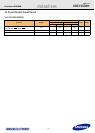
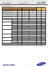
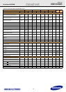
16. Timing Parameters by Speed Grade
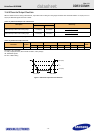
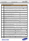
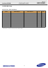
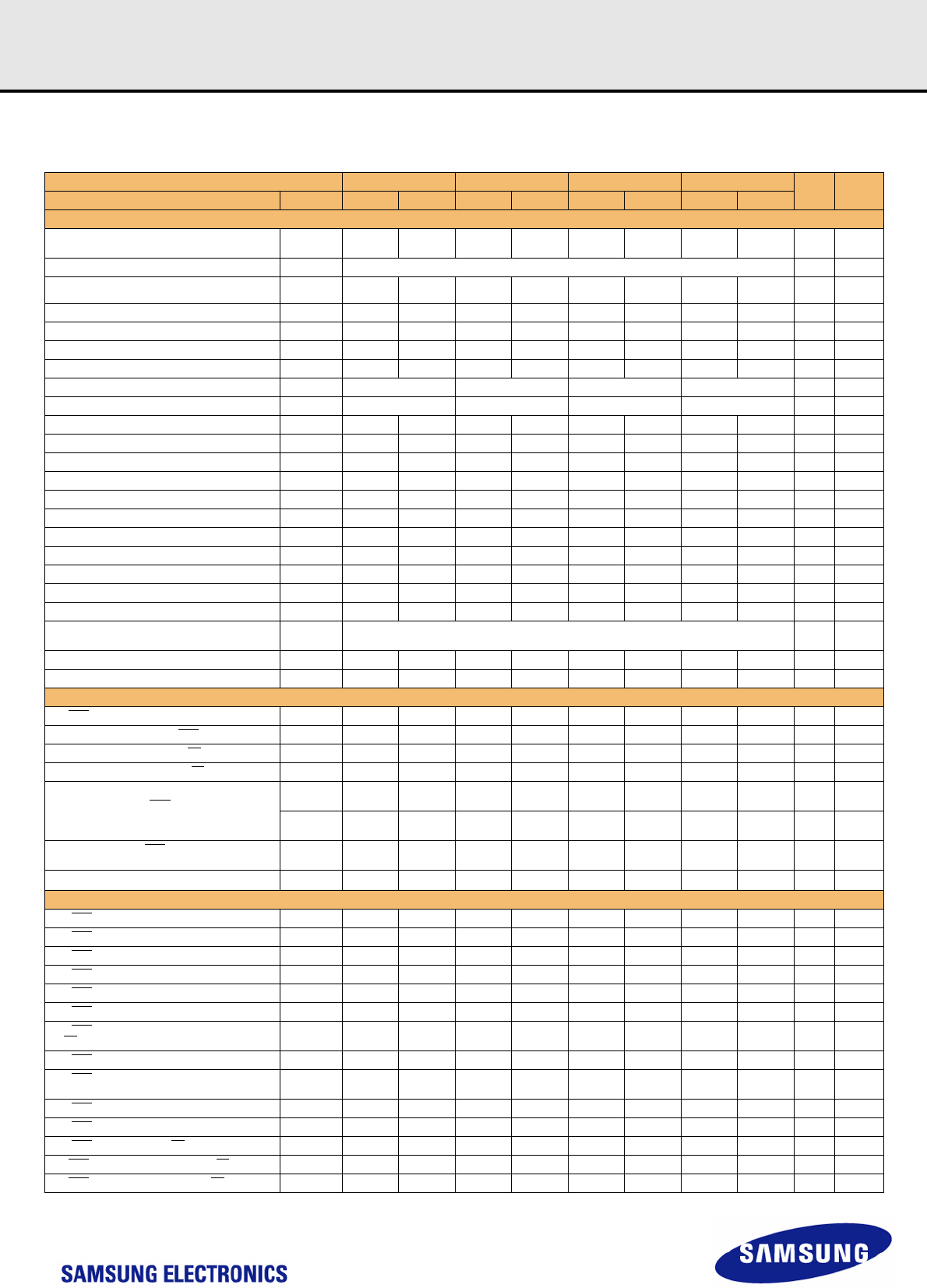
[ Table 17 ] Timing Parameters by Speed Bin
Speed DDR3-800 DDR3-1066 DDR3-1333 DDR3-1600
Units NOTE
Parameter Symbol MIN MAX MIN MAX MIN MAX MIN MAX
Clock Timing
Minimum Clock Cycle Time (DLL off mode)
tCK(DLL_OF
F)
8 - 8 - 8 - 8 - ns 6
Average Clock Period tCK(avg) See Speed Bins Table ps
Clock Period tCK(abs)
tCK(avg)min +
tJIT(per)min
tCK(avg)max +
tJIT(per)max
tCK(avg)min +
tJIT(per)min
tCK(avg)max +
tJIT(per)max
tCK(avg)min +
tJIT(per)min
tCK(avg)max +
tJIT(per)max
tCK(avg)min +
tJIT(per)min
tCK(avg)max +
tJIT(per)max
ps
Average high pulse width tCH(avg) 0.47 0.53 0.47 0.53 0.47 0.53 0.47 0.53 tCK(avg)
Average low pulse width tCL(avg) 0.47 0.53 0.47 0.53 0.47 0.53 0.47 0.53 tCK(avg)
Clock Period Jitter tJIT(per) -100 100 -90 90 -80 80 -70 70 ps
Clock Period Jitter during DLL locking period tJIT(per, lck) -90 90 -80 80 -70 70 -60 60 ps
Cycle to Cycle Period Jitter tJIT(cc) 200 180 160 140 ps
Cycle to Cycle Period Jitter during DLL locking period tJIT(cc, lck) 180 160 140 120 ps
Cumulative error across 2 cycles tERR(2per) - 147 147 - 132 132 - 118 118 -103 103 ps
Cumulative error across 3 cycles tERR(3per) - 175 175 - 157 157 - 140 140 -122 122 ps
Cumulative error across 4 cycles tERR(4per) - 194 194 - 175 175 - 155 155 -136 136 ps
Cumulative error across 5 cycles tERR(5per) - 209 209 - 188 188 - 168 168 -147 147 ps
Cumulative error across 6 cycles tERR(6per) - 222 222 - 200 200 - 177 177 -155 155 ps
Cumulative error across 7 cycles tERR(7per) - 232 232 - 209 209 - 186 186 -163 163 ps
Cumulative error across 8 cycles tERR(8per) - 241 241 - 217 217 - 193 193 -169 169 ps
Cumulative error across 9 cycles tERR(9per) - 249 249 - 224 224 - 200 200 -175 175 ps
Cumulative error across 10 cycles tERR(10per) - 257 257 - 231 231 - 205 205 -180 180 ps
Cumulative error across 11 cycles tERR(11per) - 263 263 - 237 237 - 210 210 -184 184 ps
Cumulative error across 12 cycles tERR(12per) - 269 269 - 242 242 - 215 215 -188 188 ps
Cumulative error across n = 13, 14 ... 49, 50 cycles tERR(nper)
tERR(nper)min = (1 + 0.68ln(n))*tJIT(per)min
tERR(nper)max = (1 = 0.68ln(n))*tJIT(per)max
ps 24
Absolute clock HIGH pulse width tCH(abs) 0.43 - 0.43 - 0.43 - 0.43 - tCK(avg) 25
Absolute clock Low pulse width tCL(abs) 0.43 - 0.43 - 0.43 - 0.43 - tCK(avg) 26
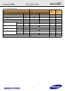
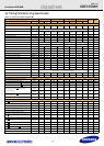
Data Timing
DQS,DQS to DQ skew, per group, per access tDQSQ - 200 - 150 - 125 - 100 ps 13
DQ output hold time from DQS, DQS tQH 0.38 - 0.38 - 0.38 - 0.38 - tCK(avg) 13, g
DQ low-impedance time from CK, CK tLZ(DQ) -800 400 -600 300 -500 250 -450 225 ps 13,14, f
DQ high-impedance time from CK, CK tHZ(DQ) - 400 - 300 - 250 - 225 ps 13,14, f
Data setup time to DQS, DQS referenced to
V
IH
(AC)V
IL
(AC) levels
tDS(base)
AC175
75
-
25
-
- - - ps d, 17
tDS(base)
AC150
125
-
75
-
30 - 10 ps d, 17
Data hold time to DQS, DQS referenced to
V
IH
(AC)V
IL
(AC) levels
tDH(base)
DC100
150
-
100
-
65 - 45 ps d, 17
DQ and DM Input pulse width for each input tDIPW 600
-
490
-
400
-
360 ps 28
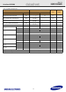
Data Strobe Timing
DQS, DQS differential READ Preamble tRPRE 0.9 NOTE 19 0.9 NOTE 19 0.9 NOTE 19 0.9 NOTE 19 tCK 13, 19, g
DQS, DQS differential READ Postamble tRPST 0.3 NOTE 11 0.3 NOTE 11 0.3 NOTE 11 0.3 NOTE 11 tCK 11, 13, b
DQS, DQS differential output high time tQSH 0.38 - 0.38 - 0.4 - 0.4 - tCK(avg) 13, g
DQS, DQS differential output low time tQSL 0.38 - 0.38 - 0.4 - 0.4 - tCK(avg) 13, g
DQS, DQS differential WRITE Preamble tWPRE 0.9 - 0.9 - 0.9 - 0.9 - tCK
DQS, DQS differential WRITE Postamble tWPST 0.3 - 0.3 - 0.3 - 0.3 - tCK
DQS, DQS rising edge output access time from rising
CK, CK
tDQSCK -400 400 -300 300 -255 255 -225 225 ps 13,f
DQS, DQS low-impedance time (Referenced from RL-1) tLZ(DQS) -800 400 -600 300 -500 250 -450 225 ps 13,14,f
DQS, DQS high-impedance time (Referenced from
RL+BL/2)
tHZ(DQS) - 400 - 300 - 250 - 225 ps 12,13,14
DQS, DQS differential input low pulse width tDQSL 0.45 0.55 0.45 0.55 0.45 0.55 0.45 0.55 tCK 29, 31
DQS, DQS differential input high pulse width tDQSH 0.45 0.55 0.45 0.55 0.45 0.55 0.45 0.55 tCK 30, 31
DQS, DQS rising edge to CK, CK rising edge tDQSS -0.25 0.25 -0.25 0.25 -0.25 0.25 -0.27 0.27 tCK(avg) c
DQS,DQS falling edge setup time to CK, CK rising edge tDSS 0.2 - 0.2 - 0.2 - 0.18 - tCK(avg) c, 32
DQS,DQS falling edge hold time to CK, CK rising edge tDSH 0.2 - 0.2 - 0.2 - 0.18 - tCK(avg) c, 32