


- 6 -
Unbuffered SODIMM datasheet DDR3 SDRAM
Rev. 1.0
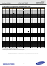
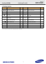
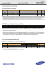
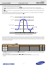
5. Pin Description
NOTE:
* The V
DD
and V
DDQ
pins are tied common to a single power-plane on these designs.
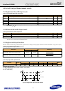
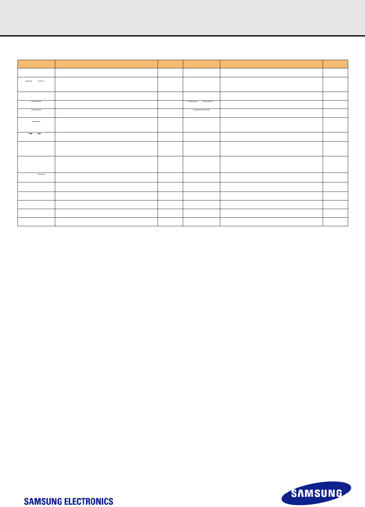
Pin Name Description Number Pin Name Description Number
CK0, CK1 Clock Inputs, positive line 2 DQ0-DQ63 Data Input/Output 64
CK
0, CK1 Clock Inputs, negative line 2 DM0-DM7
Data Masks/ Data strobes,
Termination data strobes
8
CKE0, CKE1 Clock Enables 2 DQS0-DQS7 Data strobes 8
RAS
Row Address Strobe 1 DQS0-DQS7 Data strobes complement 8
CAS
Column Address Strobe 1 RESET Reset Pin 1
WE
Write Enable 1 TEST
Logic Analyzer specific test pin (No connect
on SODIMM)
1
S
0, S1 Chip Selects 2
V
DD
Core and I/O Power 18
A0-A9, A11,
A13-A15
Address Inputs 14
V
SS
Ground 52
A10/AP Address Input/Autoprecharge 1
V
REFDQ
V
REFCA
Input/Output Reference 2
A12/BC
Address Input/Burst chop 1
V
DDSPD
SPD and Temp sensor Power 1
BA0-BA2 SDRAM Bank Addresses 3
V
TT
Termination Voltage 2
ODT0, ODT1 On-die termination control 2 NC Reserved for future use 3
SCL Serial Presence Detect (SPD) Clock Input 1 Total 204
SDA SPD Data Input/Output 1
SA0-SA1 SPD Address 2