Ultra Fast USB 2.0 Multi-Slot Flash Media Controller
Datasheet
Revision 1.1 (05-29-08) 16 SMSC USB2250/50i/51/51i
DATASHEET
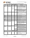
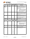
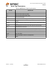
Crystal
Input/External
Clock Input
XTAL1
(CLKIN)
124 ICLKx 24MHz Crystal or external clock input.
XTAL: This pin can be connected to one
terminal of the crystal or it can be connected
to an external 24/48MHz clock when a
crystal is not used.
Note: The MA[1:0] pins will be sampled
while nRESET is asserted, and the
value will be latched upon nRESET
negation. This will determine the
clock source and value.
Crystal Output XTAL2 123 OCLKx 24MHz Crystal.
This is the other terminal of the crystal, or it
is left open when an external clock source is
used to drive XTAL1(CLKIN). It may not be
used to drive any external circuitry other than
the crystal circuit.
1.8V PLL Power VDD18PLL 125 This pin is the 1.8V Power for the PLL.
If the internal regulator is enabled, then this
pin must have a 1.0
μF (or greater) ±20%
(ESR <0.1Ω) capacitor to VSS.
3.3V Analog
Power
VDDA33 128 3.3V Analog Power
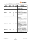
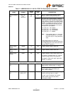
MEMORY / IO INTERFACE
Memory Data
Bus
MD[7:0] 33
29
30
31
34
35
36
37
I/O12 These signals are used to transfer data
between the internal CPU and the external
program memory.
Note: These pins have internal weak pull-
up resistors that are controlled by
the MD_PU_DIS bit of the
PWR_MGMT_CTL1 register.
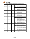
Memory Address
Bus
MA16 28 O12 These signals address memory locations
within the external memory. MA16 is a bit
generated by the ROM Mapper.
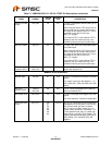
Memory Address
Bus
MA[15:2] 2
4
107
1
113
24
111
109
106
108
110
112
114
116
O12 These signals address memory locations
within the external memory.
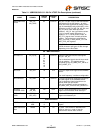
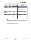
Table 5.1 USB2250/50i/51/51i 128-Pin VTQFP Pin Descriptions (continued)
NAME SYMBOL
128-PIN
VTQFP
BUFFER
TYPE DESCRIPTION


