– 16 –
CXP854P60
(6) I
2
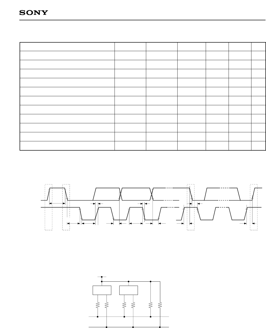
C bus timing (Ta = –10 to +75°C, VDD = 4.5 to 5.5V, Vss = 0V)
Item
SCL clock frequency
Bus free time before starting transfer
Hold time for starting transfer
Clock low level width
Clock high level width
Set-up time for repeated transfers
Data hold time
Data set-up time
SDA, SCL rise time
SDA, SCL fall time
Set-up time for transfer completion
f
SLC
tBUF
tHD; STA
tLOW
tHIGH
tSU; STA
tHD; DAT
tSU; DAT
tR
tF
tSU; STO
SCL
SDA, SCL
SDA, SCL
SCL
SCL
SDA, SCL
SDA, SCL
SDA, SCL
SDA, SCL
SDA, SCL
SDA, SCL
0
4.7
4.0
4.7
4.0
4.7
0
∗
0.25
4.7
100
1
0.3
kHz
µs
µs
µs
µs
µs
µs
µs
µs
µs
µs
Symbol Pin Condition Min. Max. Unit
∗
Since SCL rise time (max: 300ns) is not considered part of data hold time, allow at least 300ns.
Fig. 9. I
2
C bus transfer data timing
PSt
tSU; STO
tSU; STA
tHD; STA
tSU; DATtHIGHtHD; DAT
tFtR
tLOW
tHD; STA
SP
t
BUF
SDA
SCL
Fig. 10. I
2
C device suggested circuit
I
2
C
device
I
2
C
device
RS RS RS RS RP RP
SDA0
(or SDA1)
SCL0
(or SCL1)
• A pull-up resistor must be connected to SDA0 (or SDA1), and SCL0 (or SCL1).
• The SDA0 (or SDA1) and SCL0 (or SCL1) series resistance (Rs = 300Ω or less) can be used to reduce spike
noise caused by CRT flashover.


