


360050398
Toshiba Corporation Digital Media Network Company
Page 50 of 157
© 2005, Copyright TOSHIBA Corporation All Rights Reserved
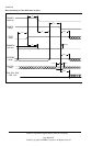
10.6 Address Decoding
The host addresses the drive using programmed I/O. In this method, the required register address should
be placed on the three host address lines, DA2 - DA0. An appropriate chip is selected and a read or write
strode (-DIOR / -DIOW) shall be given to the chip.
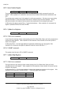
The following I/O map shows definitions of all the register addresses and functions for these I/O locations.
The descriptions of each register are shown in the next paragraph.
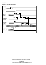
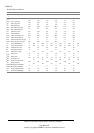
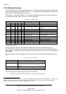
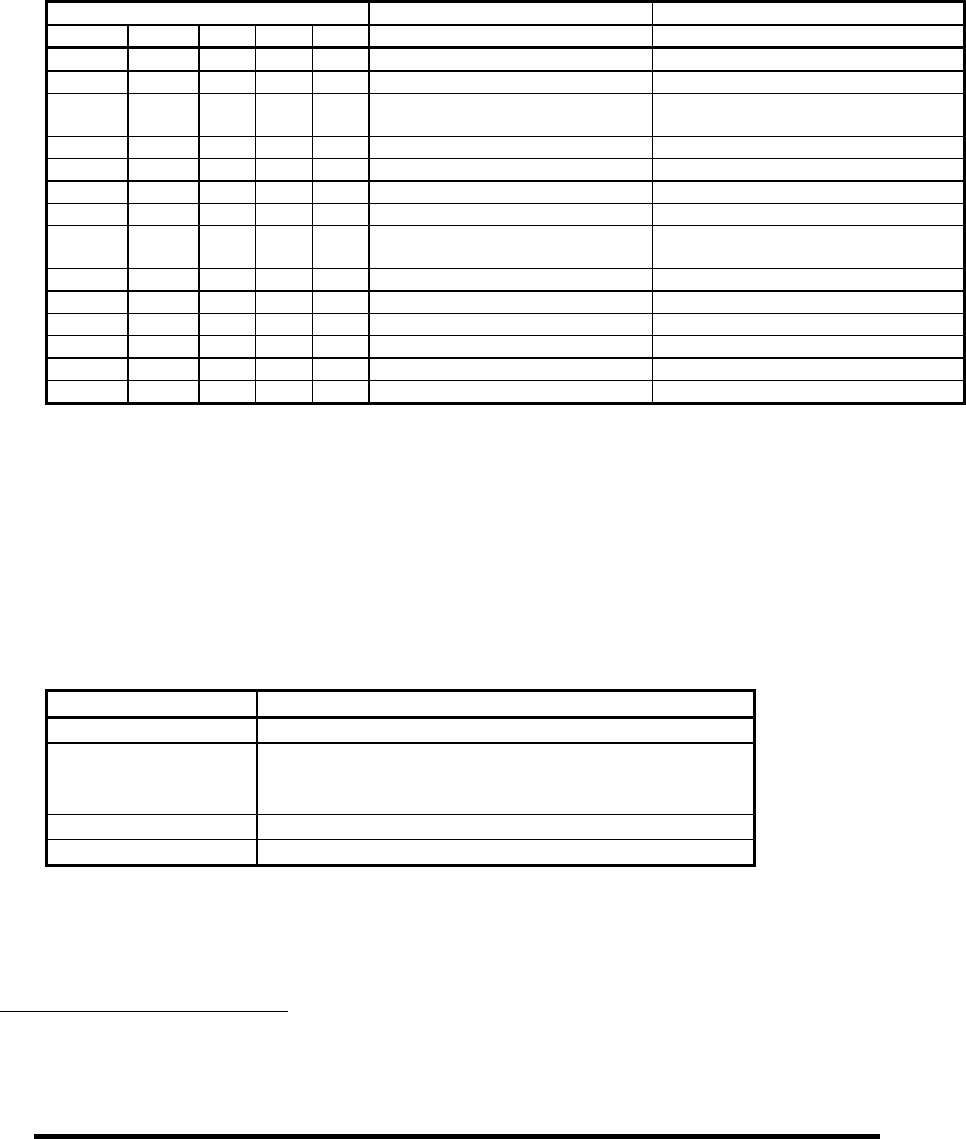
Table 10.6-1 Register map
Address
- CS0 - CS1 HA2 HA1 HA0 READ REGISTER WRITE REGISTER
0 0 X X X Invalid address Invalid address
0 1 0 0 0 Data register Data register
0 1 0 0 1 Error register Features (Write precompensation)
register
0 1 0 1 0 Sector count Sector count
0 1 0 1 1 Sector number / LBA bit 0- 7 Sector number / LBA bit0-7
0 1 1 0 0 Cylinder low / LBA bit 8- 15 Cylinder low / LBA bit8-15
0 1 1 0 1 Cylinder high / LBA bit16- 23 Cylinder high / LBA bit16-23
0 1 1 1 0 Device head register
/ LBA bit 24- 27
Device head register
/ LBA bit 24-27
0 1 1 1 1 Status register Command register
1 0 0 X X High impedance Not used
1 0 1 0 X High impedance Not used
1 0 1 1 0 Alt. status register Device control register
1 0 1 1 1 Device address register
1
Not used
1 1 X X X High impedance Not used
“X” means “don't care”.
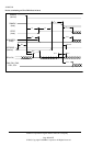
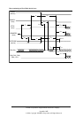
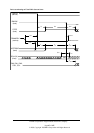
The host generates selection of two independent chips on the interface. The selected high order
chip ,-HOST CS1, is valid only when the host is accessing the address of alternate status register, digital
output register , and digital input register respectively. The low order chip, HOST CS0, is used to address all
other registers.
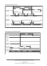
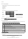
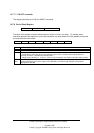
The following table shows the standard decode logic to connect with ISA (Industry Standard Architecture)
bus .
Table 10.6-2 Decode Logic
Register Address Map Decode
1F0-1F7 - CS0 = - ((- A9) (-A3)*(- AEN))
3F6,3F7 - CS1= -
(A9*A8*A7*A6*A5*A*A8*A7*A6*A5*A4*4)*(-A3)*(-
AEN)
170-177 - CS0= - ((- A9)*A8*(- A7)*A6*A5*A4*(- A3)*(- AEN)
376,377 - CS1= - (A9*A8*(- A7)*A6*A5*A4)*(- A3)*(- AEN)
The host data buses 15-8 are valid only when - IOCS16 is active.
• - IOCS16 is asserted when interface address lines match to data register address.
1
ATA-2 Notes: This register is obsolete. A device is not supposed to respond to a read of this address. If a device does
respond, it shall be sure not to drive the DD7 signal to prevent possible conflict with floppy disk implementations.
The drive supports this register to maintain compatibility for ATA-1.