


TMP92CZ26A
92CZ26A-351
3.15.5 Control in I
2
C Bus Mode
(1) Acknowledge Mode Specification
When slave address is matched or detecting GENERAL CALL, and set the
SBICR1<ACK> to “1”, TMP92CZ26A operates in the acknowledge mode. The
TMP92CZ26A generates an additional clock pulse for an Acknowledge signal when
operating in Master Mode. In the transmitter mode during the clock pulse cycle, the
SDA pin is released in order to receive the acknowledge signal from the receiver. In
the receiver mode during the clock pulse cycle, the SDA pin is set to the Low in order
to generate the acknowledge signal.
Clear the <ACK> to “0” for operation in the Non-Acknowledge Mode; The
TMP92CZ26A does not generate a clock pulse for the Acknowledge signal when
operating in the Master Mode.
(2) Number of transfer bits
The SBICR1<BC2:0> is used to select a number of bits for next transmitting and
receiving data.
Since the <BC2:0> is cleared to 000 as a start condition, a slave address and direction
bit transmission are executed in 8 bits. Other than these, the <BC2:0> retains a
specified value.
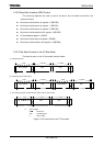
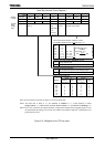
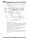
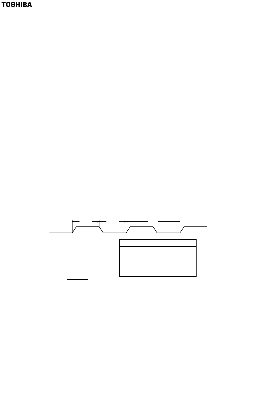
(3) Serial clock
a. Clock source
The SBICR1 <SCK2:0> is used to select a maximum transfer frequency outputted
on the SCL pin in Master Mode. Set the baud rates, which have been calculated
according to the formula below, to meet the specifications of the I2C bus, such as the
smallest pulse width of t
LOW,
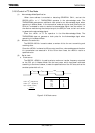
Figure 3.15.8 Clock source
t
HIGH
t
LOW
1/fscl
t
LOW
= (2
n-1
+ 29)/(f
SYS
/4)
t
HIGH
= (2
n
−
1
+ 6)/(f
SYS
/4)
fscl = 1/(t
LOW
+ t
HIGH
)
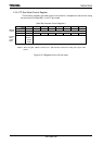
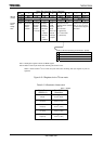
SBICR1<SCK2:0> n
000 4
001 5
010 6
011 7
100 8
101 9
110 10
=
f
SYS
/4
2
n
+ 35