


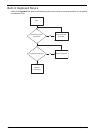
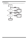
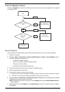
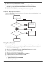
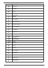
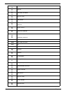

156 Chapter 4
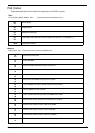
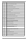
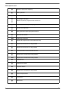
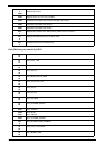
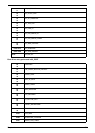
0x
14
Verify burst length of 8 is supported by all DIMMs
0x
15
Determine the smallest tWR supported by all DIMMs
0x
16
Determine DIMM size parameters
0x
17
Program the correct system memory frequency
0x
18
Determine and set the mode of operation for the memory channels
0x
19
Program clock crossing registers
0x
20
Disable Fast Dispatch
0x
21
Program the DRAM Row Attributes and DRAM Row Boundary registers
0x
22
Program the DRAM Bank Architecture register
0x
23
Program the DRAM Timing & and DRAM Control registers
0x
24
Program ODT
0x
25
Perform steps required before memory init
0x
26
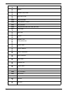
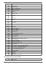
Program the receive enable reference timing control register
Program the DLL Timing Control Registers, RCOMP settings
0x
27
Enable DRAM Channel I/O Buffers
0x
28
Enable all clocks on populated rows
0x
29
Perform JEDEC memory initialization for all memory rows
0x
30
0x
31
Perform steps required after memory init
Program DRAM throttling and throttling event registers
0x
32
Setup DRAM control register for normal operation and enable
0x
33
Enable RCOMP
0x
34
Clear DRAM initialization bit in the SB
0x
35
Initialization Sequence Completed, program graphic clocks
0x
AF
Disable access to the XMM registers