48
Regulation & Control Subsystem
This sub-system may be considered to be the brains of the unit. It provides the control pulses to open and close the
switching elements which deliver power to the output. This section also regulates the output to ensure that the unit is
delivering a constant power at either a constant voltage or constant current setting. In the event that this cannot be achieved,
then the protection subsystem is employed to limit the power to the output.
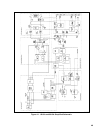
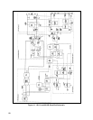
To understand how this control is achieved, consider Figure 4-1, the simplified schematic. Power from the output is
sampled and attenuated before it is fed back to the Constant Voltage Error Amplifier. Another input to this amplifier is the
Program Voltage which the user sets via the front panel. The difference between these two voltages is amplified and
becomes the CV Error Signal. The output of the supply is also sampled by the CC Monitor Amp. This sample voltage is fed
into the Constant Current Error Amp. The other input to the Constant Current Error Amp is the program current which the
user sets via the front panel. The difference between these two voltages is amplified and becomes the Constant Current
Error Signal. These two signals are connected in a wired-OR configuration and fed into the Constant Voltage Comparator.
The control mechanism which the unit employs to regulate its output comprises the Primary Current Monitor Transformer,
the Control Voltage Comparator and the Pulse Width Modulator. The Primary Current Monitor Transformer senses the
power transferred by the FETs and generates the Ip Ramp Voltage which continues to build up as the output increases. This
Ramp Voltage and the Control Voltage are used as inputs to the control voltage Comparator. If the Ramp Voltage exceeds
the Control Voltage, the output of the comparator goes low and resets the Pulse Width Modulator in the process. If the unit
develops power in excess of its requirements, the power LIMIT Comparator effectively monitors this condition and returns
a low signal which disables the Pulse Width Modulator and prevents any further power development.
The PULSE WIDTH Modulator (PWM) is the device which the unit employs to constantly alter the duty cycle of the
switching waveform produced by the FETs. Once reset, it triggers the off-pulse one-shot which turns off the FETs via the
off-pulse driver. The 20KHz entering the PWM holds it reset for 1.5
µS and on the next clock pulse from the oscillator the
output is clocked high. This in turn triggers the on-pulse one-shot which enables the FETs. Other inputs which can disable
the PWM are the outputs from the Power Limit Comparator, the Master Enable, the CV and CC loop.
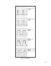
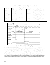
Figure 4-2 shows the timing diagram of the signals which control the FETs. Notice that on the rising edge of the on-pulse,
the PWM is activated and remains on until the off pulse is sent. There is a slight delay in the time the off-pulse is sent and
the time the FETs are actually turned off. This turn off delay results in greater power being generated than is required as
shown by the Ramp Voltage exceeding the Control Voltage. To prevent this situation, there is an Initial Ramp Circuit
which increases the Ramp Voltage and enables the voltage to ramp up to the Control Voltage level earlier.
The sampled output voltage is fed back through the Constant Voltage Circuit and the Constant Current Circuit before it
becomes the Control Voltage. The CV and CC circuits provide the means for the instrument to deliver power at either
constant voltage or constant current.
The CONSTANT VOLTAGE circuit takes its input from two positions on the output voltage rail: the Innerloop Voltage
Sense (IVS), and the outerloop Voltage Sense (OVS) at the + S and - S terminals. The CV Monitor Amplifier attenuates the
OVS in the ratio of 1:40 (6010A); 1:4 (6011A); 1:12 (6012B); 1:100 (6015A), and produces the Voltage Monitor(V-MON)
signal. This signal connects through protective circuitry to the rear panel and display circuits on the front panel, and also
forms the input to the CV Error Amplifier. The Program Voltage which the user sets at the front panel voltage control is
also an input to this amplifier. The output is the error signal which together with the output from the Innerloop Voltage
Sense (IVS) generates the CV Control Voltage.
In addition to the Front Panel settings, the CV Program Voltage can be set from an external voltage applied between rear
panel terminals VP and
P, or from an external resistor between these same terminals.


