Panel and Jumper Definition
10
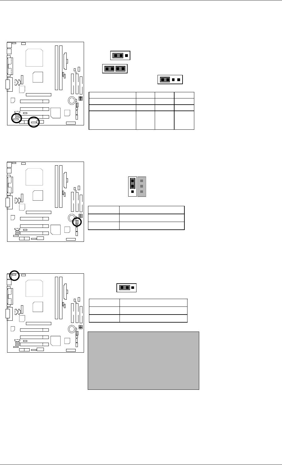
J16 /J17/J18: CNR (Primary or Secondary) Select [Optional]
(CNR Communication and Networking Riser)
J16 J17 J18
Onboard AC97 1-2 1-2 1-2
CNR (Primary) 2-3 3-4 3-4
Onboard AC97 CNR
(Secondary)
[Optional]
1-2 1-2
3-4
1-2
1
J16
1
J17
1
J18
JP3: Clear CMOS Function (Optional)
Pin No. Definition
1-2 close Normal (Default)
2-3 close Clear CMOS
1
JP4: USB Device Wake up Selection
Pin No. Definition
1-2 close Normal (Default)
2-3 close USB Device Wake up
1
(If you want to use “USB Dev Wakeup from S3~S5”
function, you have to set the BIOS setting “USB Dev
Wakeup from S3~S5” enabled, and the jumper “JP4”
enabled)
*(Power on the computer and as soon as memory
counting starts, press <Del>. You will enter BIOS Setup.
Select the item “POWER MANAGEMENT SETUP”,
then select “USB Dev Wakeup from S3~S5”.
Remember to save the setting by pressing "ESC" and
choose the “SAVE & EXIT SETUP” option.)


