


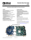

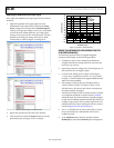
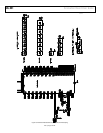

Evaluation Board User Guide UG-001
Rev. 0 | Page 5 of 24
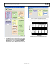
DEFAULT OPERATION AND
JUMPER SELECTION SETTINGS
This section explains the default and optional settings or modes
allowed on the AD9272/AD9273 Rev. A evaluation board.
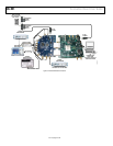
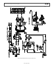
Power Circuitry
Connect the switching power supply that is supplied in the
evaluation kit between a rated 100 V ac to 240 V ac wall outlet
at 47 Hz to 63 Hz and P701.
Analog Input Front-End Circuit
The evaluation board is set up for a transformer-coupled analog
input with an optimum 50 Ω impedance match of 18 MHz of
bandwidth. For a different bandwidth response, use the
antialiasing filter settings.
VREF
VREF is set to 1.0 V. This causes the ADC to operate with the
internal reference in the 2.0 V p-p full-scale range. A separate
external reference option using the ADR130 is also included on
the evaluation board. Populate R311 with a 0 Ω resistor and remove
C426. Note that ADC full-scale ranges less than 2.0 V p-p are
not supported by the AD9272/AD9273.
RBIAS
RBIAS has a default setting of 10 kΩ (R301) to ground and is used
to set the ADC core bias current. However, note that using other
than a 10 kΩ, 1% resistor for RBIAS may degrade the performance
of the device, depending on the resistor chosen.
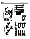
Clock Circuitry
The default clock input circuitry is derived from a sim-
ple transformer-coupled circuit using a high bandwidth
1:1 impedance ratio transformer (T401) that adds a very low
amount of jitter to the clock path. The clock input is 50 Ω
terminated and ac-coupled to handle single-ended sine wave
types of inputs. The transformer converts the single-ended
input to a differential signal that is clipped before entering the
ADC clock inputs.
The evaluation board is already set up to be clocked from the
crystal oscillator, OSC401. This oscillator is a low phase noise
oscillator from Valpey Fisher (VFAC3-BHL-50MHz/VFAC3-
BHL-65MHz/VFAC3-BHL-80MHz). If a different clock source
is desired, remove R403, set Jumper J401 to disable the oscillator
from running, and connect the external clock source to the
SMA connector, P401.
A differential LVPECL clock driver can also be used to clock the
ADC input using the AD9515 (U401). Populate R406 and R407
with 0 Ω resistors and remove R415 and R416 to disconnect the
default clock path inputs. In addition, populate C405 and C406
with a 0.1 μF capacitor and remove C409 and C410 to disconnect
the default clock path outputs. The AD9515 has many pin-
strappable options that are set to a default mode of operation.
Consult the AD9515 data sheet for more information about
these and other options.
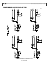
PDWN
To enable the power-down feature, short P303 to the on
position (AVDD) on the PDWN pin.
STBY
To enable the standby feature, short P302 to the on position
(AVDD) on the STBY pin.
GAIN+, GAIN−
To change the VGA attenuation, drive the GAIN+ pin from 0 V
to 1.6 V on J302 using a linear supply and use a single-ended
method to change the VGA gain from 0 dB to 42 dB. U403 is
available for users who wish to drive the gain pins (GAIN±)
differentially. Install R305, R347, and R349 and remove C308,
C309, and R303 to connect the amplifier correctly. Next, apply a
dc voltage source to P601, connecting the +5 V, −5 V, and ground
(0 V) appropriately to bias U403 (AD8138). These benchtop
linear supplies should each have 100 mA of current capability.
If an external source is not available, R337 can be installed to
use the on-board resistive divider for gain adjustment in either
the single-ended or differential case.
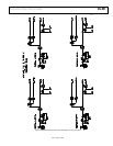
Non-SPI Mode
For users who wish to operate the DUT without using SPI,
remove the jumpers on J601. This disconnects the CSB, SCLK,
and SDIO pins from the control bus, allowing the DUT to
operate in its simplest mode. Each of these pins has internal
termination and will float to its respective level. Note that the
device will only work in its default condition.
CWDx+, CWDx−
To use the CWDx± outputs, first apply a dc voltage source to
P601, connecting the +5 V, −5 V, and ground (0 V) appropriately to
bias U402 (AD812). These benchtop linear supplies should each
have 100 mA of current capability.
To view the CWD2+/CWD2− through CWD5+/CWD5− outputs,
jumper together the appropriate outputs on P606 and P607. All
outputs are summed together on the IOP and ION buses, fed to
a 1:4 impedance ratio transformer, and buffered so that the user
can view the output on a spectrum analyzer. This can be configured
to be viewed in single-ended mode (default) or in differential mode
by using a spectrum analyzer. To set the voltage for the appropriate
number of channels to be summed, change the value of R447
and R448 on the primary transformer (T402).
Upon shipment, the CWD0+/CWD0−, CWD1+/CWD1−,
CWD6+/CWD6−, and CWD7+/CWD7− outputs are properly
biased and ready to use with the AD8339 quad I/Q demodulator
and phase shifter. The AD9272/AD9273 evaluation board simply
snaps into place on the AD8339 evaluation board (AD8339-
EVALZ). Remove the jumpers connected to P3A and P4A on
the AD8339 evaluation board, and snap the standoffs that are
provided with the AD9272/AD9273 into the AD8339 evaluation
board standoff holes in the center of the board. The standoffs
will automatically lock into place and create a direct connection