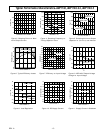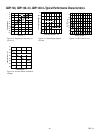
ADP1148, ADP1148-3.3, ADP1148-5
–7–
REV. A
APPLICATIONS
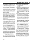
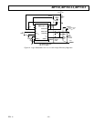
The ADP1148 uses a current-mode, constant off-time structure
to switch a pair of external complementary N- and P-channel
MOSFETs. The operating frequency of the device is deter-
mined by the value of the external capacitor connected to the
C
T
pin.
The output voltage is sensed by an internal voltage divider which is
connected to the Sense(–) pin (ADP1148-3.3 and AD1148-5) or
an external voltage divider returned to V
FB
(ADP1148). A voltage
comparator V, and a gain block G compare the values of the
divided output voltage with a reference voltage of 1.25 V.
To maximize the efficiency, the ADP1148 automatically switches
between two operational modes, power-saving and continuous.
The Flip-Flop 1 is the main control element when the device is
in its power-saving mode while the gain block is the main con-
trol when the output voltage moves to continuous mode. During
the continuous mode of the PMOS switch on-cycle, the current
comparator C, monitors the voltage between Sense(–) and
Sense(+). When the voltage level reaches the threshold level, the
P drive output is switched to V
IN
which turns off the P-channel
MOSFET. The timing capacitor C
T
is now able to discharge at
a rate determined by the off-time controller. The discharge
current is made to be proportional to the value of the output
voltage (measured at the Sense(–) pin) to model the inductor
current which decays at a rate which is proportional to the out-
put voltage. While the timing capacitor is discharging, the N
drive output goes to V
IN
, turning on the N-channel MOSFET.
When the voltage level on the timing capacitor has discharged to
the threshold voltage level V
TH1
, comparator T switches setting
Flip-Flop 1. This forces the N drive to go off and the P drive
output low and subsequently turns the P-channel MOSFET on.
The sequence is then repeated. As load current increases, the
output voltage starts to reduce. This results in the output of the
gain circuit increasing the level of the current comparator thresh-
old, thus tracking the load current.
At very low load currents the power-saving sequence will be
interrupted by the Set of Flip-Flop 2, by voltage comparator B,
which also monitors the voltage across R
SENSE
. When the load
current decreases to half the designed inductor ripple current,
the voltage across R
SENSE
will reverse polarity. When this hap-
pens, comparator B will set the Q-bar output of Flip-Flop 2,
which will go to logic zero state and interrupt the cycle-by-cycle
operation and inhibit the output FET-driver. The output of the
power supply storage capacitor will slowly be drained by the
load and the output voltage starts decreasing. When this
decreased voltage exceeds the V
OS
of comparator V, this in turn
will reset Flip-Flop 2, and normal cycle-by-cycle operation will
resume. If the load is very small, it will take a long time for Flip-
Flop 2 to reset, and during that time the oscillator capacitor
may discharge below V
TH2
. At the point at which the timing
capacitor discharges below V
TH2
, comparator S trips causing the
internal sleep-bar to go low. The circuit is now in sleep mode
and the N-channel Power MOSFET remains turned off. While
the circuit remains in this mode, a significant amount of the
circuit of the IC is turned off dropping the ground current from
approximately 1.6 mA to a level of 160 µA. In this state the load
current is supplied by the output capacitor. The sleep mode is
also terminated by the reset of Flip-Flop 2.
To prevent both the external MOSFETs from ever being turned
on simultaneously, feedback is incorporated to sense the state of
the driver output pins.
Before the N drive output can go high, the P drive output must
also be high. Likewise, the P drive output is unable to go low
while the N drive output is high. By utilizing a constant off-time
structure, the device operation is a function of the input voltage.
To limit the effect of frequency variation as the device approaches
dropout, the controller begins to increase the discharge current
as V
IN
drops below V
OUT
+1.5 V. While the device is in drop-
out, the P-channel MOSFET is on constantly.
R
SENSE
Selection For Output Current
The choice of R
SENSE
is based on the required output current.
The ADP1148 current comparator has a threshold range which
extends from 0 mV to a maximum of 150 mV/R
SENSE
. The
current comparator threshold sets the peak of the inductor cur-
rent, yielding a maximum output current I
MAX
equal to the peak
value less half the peak-to-peak ripple current. The ADP1148
operates effectively with values of R
SENSE
from 20 mΩ to
200 mΩ. A graph for selecting R
SENSE
versus maximum output
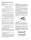
current is given in Figure 3. Solving for R
SENSE
and allowing a
margin for variations in the ADP1148 and external component
values yields:
R
SENSE
= 100 mV/I
MAX
The peak short circuit current, (I
SC(PK)
) tracks I
MAX
. Once
R
SENSE
has been chosen, I
SC(PK)
can be predicted from the fol-
lowing equation:
I
SC(PK)
= 150 mV/R
SENSE
The load current, below which power-saving mode commences
(I
POWER-SAVING
) is determined by the offset in comparator B and
the value of the inductor chosen. Comparator B is designed to
have approximately 5 mV offset. This offset and the inductor
can now be used to predict the power saving mode current as
follows:
I
POWER-SAVING
~ 5 mV/R
SENSE
+ V
O
× t
OFF
/2 L
The ADP1148 automatically extends t
OFF
during a short circuit
to provide adequate time for the inductor current to decay be-
tween switch cycles. The resulting ripple current causes the
average short circuit current, I
SC(AVG)
, to be lowered to approxi-
mately I
MAX
.
L and C
T
Selection for Operating Frequency
The ADP1148 uses a constant off-time architecture with t
OFF
determined by an external timing capacitor C
T
. Each time the
P-channel MOSFET switch turns on, the voltage on C
T
is reset
to approximately 3.3 V. During the off time, C
T
is discharged by
a current which is proportional to V
OUT
. The voltage on C
T
is
analogous to the current in inductor L, which likewise decays at
a rate proportional to V
OUT
. Therefore, the inductor value must
track the timing capacitor value.
The value of C
T
is calculated from the preferred continuous
mode operating frequency:
C
T
= 1/2.6 × 10
4
× f
Assumes V
IN
= 2 V
OUT
(Figure 1 circuit).
A graph for selecting C
T
versus frequency including the effects
of input voltage is given in Figure 5.
*Component, voltage, current, etc., values are in SI-units (international standard)
unless otherwise indicated.


